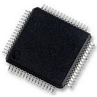
S9S12HY64J0MLH Freescale Semiconductor, S9S12HY64J0MLH Datasheet - Page 300

S9S12HY64J0MLH
Manufacturer Part Number
S9S12HY64J0MLH
Description
MCU 64K FLASH AUTO 64-LQFP
Manufacturer
Freescale Semiconductor
Series
HCS12r
Datasheet
1.S9S12HA32J0CLL.pdf
(792 pages)
Specifications of S9S12HY64J0MLH
Core Processor
HCS12
Core Size
16-Bit
Speed
32MHz
Connectivity
CAN, EBI/EMI, I²C, IrDA, LIN, SCI, SPI
Peripherals
LCD, Motor control PWM, POR, PWM, WDT
Number Of I /o
50
Program Memory Size
64KB (64K x 8)
Program Memory Type
FLASH
Eeprom Size
4K x 8
Ram Size
4K x 8
Voltage - Supply (vcc/vdd)
4.5 V ~ 5.5 V
Data Converters
A/D 6x10b
Oscillator Type
Internal
Operating Temperature
-40°C ~ 125°C
Package / Case
64-LQFP
Controller Family/series
S12
No. Of I/o's
50
Ram Memory Size
4KB
Cpu Speed
64MHz
No. Of Timers
2
Rohs Compliant
Yes
Processor Series
S12HY
Core
HCS12
3rd Party Development Tools
EWHCS12
Development Tools By Supplier
DEMO9S12HY64
Lead Free Status / RoHS Status
Lead free / RoHS Compliant
Available stocks
Company
Part Number
Manufacturer
Quantity
Price
Company:
Part Number:
S9S12HY64J0MLH
Manufacturer:
Freescale Semiconductor
Quantity:
10 000
- Current page: 300 of 792
- Download datasheet (4Mb)
Analog-to-Digital Converter (ADC12B8CV1) Block Description
8.3.2.10
Read: Anytime
Write: Anytime
8.3.2.11
Writes to this register will abort current conversion sequence.
Read: Anytime
Write: Anytime
300
Module Base + 0x000C
Module Base + 0x000E
CMPHT[7:0]
IEN[7:0]
Reset
Reset
Field
Field
7–0
7–0
W
W
R
R
15
15
0
0
0
0
ATD Digital Input Enable on channel x (x= 7, 6, 5, 4, 3, 2, 1, 0) — This bit controls the digital input buffer from
the analog input pin (ANx) to the digital data register.
0 Disable digital input buffer to ANx pin
1 Enable digital input buffer on ANx pin.
Note: Setting this bit will enable the corresponding digital input buffer continuously. If this bit is set while
ATD Input Enable Register (ATDDIEN)
ATD Compare Higher Than Register (ATDCMPHT)
Compare Operation Higher Than Enable for conversion number n (n= 7, 6, 5, 4, 3, 2, 1, 0) of a Sequence
(n conversion number, NOT channel number!) — This bit selects the operator for comparison of conversion
results.
0 If result of conversion n is lower or same than compare value in ATDDRn, this is flagged in ATDSTAT2
1 If result of conversion n is higher than compare value in ATDDRn, this is flagged in ATDSTAT2
= Unimplemented or Reserved
= Unimplemented or Reserved
14
14
0
0
0
0
simultaneously using it as an analog port, there is potentially increased power consumption because the
digital input buffer maybe in the linear region.
Figure 8-13. ATD Compare Higher Than Register (ATDCMPHT)
13
13
0
0
0
0
Figure 8-12. ATD Input Enable Register (ATDDIEN)
12
12
0
0
0
0
MC9S12HY/HA-Family Reference Manual, Rev. 1.04
Table 8-20. ATDCMPHT Field Descriptions
Table 8-19. ATDDIEN Field Descriptions
11
11
0
0
0
0
10
10
0
0
0
0
0
0
0
0
9
9
0
0
0
0
8
8
Description
Description
0
0
7
7
0
0
6
6
0
0
5
5
CMPHT[7:0]
4
0
4
0
IEN[7:0]
0
0
3
3
Freescale Semiconductor
0
0
2
2
0
0
1
1
0
0
0
0
Related parts for S9S12HY64J0MLH
Image
Part Number
Description
Manufacturer
Datasheet
Request
R
Part Number:
Description:
Manufacturer:
Freescale Semiconductor, Inc
Datasheet:
Part Number:
Description:
Manufacturer:
Freescale Semiconductor, Inc
Datasheet:
Part Number:
Description:
Manufacturer:
Freescale Semiconductor, Inc
Datasheet:
Part Number:
Description:
Manufacturer:
Freescale Semiconductor, Inc
Datasheet:
Part Number:
Description:
Manufacturer:
Freescale Semiconductor, Inc
Datasheet:
Part Number:
Description:
Manufacturer:
Freescale Semiconductor, Inc
Datasheet:
Part Number:
Description:
Manufacturer:
Freescale Semiconductor, Inc
Datasheet:
Part Number:
Description:
Manufacturer:
Freescale Semiconductor, Inc
Datasheet:
Part Number:
Description:
Manufacturer:
Freescale Semiconductor, Inc
Datasheet:
Part Number:
Description:
Manufacturer:
Freescale Semiconductor, Inc
Datasheet:
Part Number:
Description:
Manufacturer:
Freescale Semiconductor, Inc
Datasheet:
Part Number:
Description:
Manufacturer:
Freescale Semiconductor, Inc
Datasheet:
Part Number:
Description:
Manufacturer:
Freescale Semiconductor, Inc
Datasheet:
Part Number:
Description:
Manufacturer:
Freescale Semiconductor, Inc
Datasheet:
Part Number:
Description:
Manufacturer:
Freescale Semiconductor, Inc
Datasheet:


