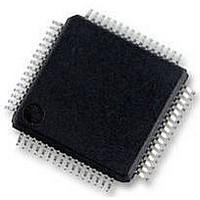
S9S12HY64J0MLH Freescale Semiconductor, S9S12HY64J0MLH Datasheet - Page 187

S9S12HY64J0MLH
Manufacturer Part Number
S9S12HY64J0MLH
Description
MCU 64K FLASH AUTO 64-LQFP
Manufacturer
Freescale Semiconductor
Series
HCS12r
Datasheet
1.S9S12HA32J0CLL.pdf
(792 pages)
Specifications of S9S12HY64J0MLH
Core Processor
HCS12
Core Size
16-Bit
Speed
32MHz
Connectivity
CAN, EBI/EMI, I²C, IrDA, LIN, SCI, SPI
Peripherals
LCD, Motor control PWM, POR, PWM, WDT
Number Of I /o
50
Program Memory Size
64KB (64K x 8)
Program Memory Type
FLASH
Eeprom Size
4K x 8
Ram Size
4K x 8
Voltage - Supply (vcc/vdd)
4.5 V ~ 5.5 V
Data Converters
A/D 6x10b
Oscillator Type
Internal
Operating Temperature
-40°C ~ 125°C
Package / Case
64-LQFP
Controller Family/series
S12
No. Of I/o's
50
Ram Memory Size
4KB
Cpu Speed
64MHz
No. Of Timers
2
Rohs Compliant
Yes
Processor Series
S12HY
Core
HCS12
3rd Party Development Tools
EWHCS12
Development Tools By Supplier
DEMO9S12HY64
Lead Free Status / RoHS Status
Lead free / RoHS Compliant
Available stocks
Company
Part Number
Manufacturer
Quantity
Price
Company:
Part Number:
S9S12HY64J0MLH
Manufacturer:
Freescale Semiconductor
Quantity:
10 000
- Current page: 187 of 792
- Download datasheet (4Mb)
6.3.2
This section consists of the DBG control and trace buffer register descriptions in address order. Each
comparator has a bank of registers that are visible through an 8-byte window between 0x0028 and 0x002F
in the DBG module register address map. When ARM is set in DBGC1, the only bits in the DBG module
registers that can be written are ARM, TRIG, and COMRV[1:0]
6.3.2.1
Read: Anytime
Write: Bits 7, 1, 0 anytime
Freescale Semiconductor
1
2
3
4
Address: 0x0020
Address
0x002E
0x002F
This bit is visible at DBGCNT[7] and DBGSR[7]
This represents the contents if the Comparator A control register is blended into this address.
This represents the contents if the Comparator B control register is blended into this address
This represents the contents if the Comparator C control register is blended into this address
Reset
W
R
Bit 6 can be written anytime but always reads back as 0.
Bits 4:3 anytime DBG is not armed.
DBGADHM
DBGADLM
Register Descriptions
ARM
Name
Debug Control Register 1 (DBGC1)
0
7
When disarming the DBG by clearing ARM with software, the contents of
bits[4:3] are not affected by the write, since up until the write operation,
ARM = 1 preventing these bits from being written. These bits must be
cleared using a second write if required.
= Unimplemented or Reserved
W
W
R
R
TRIG
0
0
6
Bit 15
Bit 7
Bit 7
Figure 6-2. Quick Reference to DBG Registers
MC9S12HY/HA-Family Reference Manual, Rev. 1.04
Figure 6-3. Debug Control Register (DBGC1)
14
0
0
5
6
6
13
5
5
BDM
NOTE
0
4
12
4
4
DBGBRK
0
3
11
3
3
0
0
2
S12S Debug Module (S12SDBGV2)
10
2
2
0
1
1
9
1
COMRV
Bit 0
Bit 8
Bit 0
0
0
187
Related parts for S9S12HY64J0MLH
Image
Part Number
Description
Manufacturer
Datasheet
Request
R
Part Number:
Description:
Manufacturer:
Freescale Semiconductor, Inc
Datasheet:
Part Number:
Description:
Manufacturer:
Freescale Semiconductor, Inc
Datasheet:
Part Number:
Description:
Manufacturer:
Freescale Semiconductor, Inc
Datasheet:
Part Number:
Description:
Manufacturer:
Freescale Semiconductor, Inc
Datasheet:
Part Number:
Description:
Manufacturer:
Freescale Semiconductor, Inc
Datasheet:
Part Number:
Description:
Manufacturer:
Freescale Semiconductor, Inc
Datasheet:
Part Number:
Description:
Manufacturer:
Freescale Semiconductor, Inc
Datasheet:
Part Number:
Description:
Manufacturer:
Freescale Semiconductor, Inc
Datasheet:
Part Number:
Description:
Manufacturer:
Freescale Semiconductor, Inc
Datasheet:
Part Number:
Description:
Manufacturer:
Freescale Semiconductor, Inc
Datasheet:
Part Number:
Description:
Manufacturer:
Freescale Semiconductor, Inc
Datasheet:
Part Number:
Description:
Manufacturer:
Freescale Semiconductor, Inc
Datasheet:
Part Number:
Description:
Manufacturer:
Freescale Semiconductor, Inc
Datasheet:
Part Number:
Description:
Manufacturer:
Freescale Semiconductor, Inc
Datasheet:
Part Number:
Description:
Manufacturer:
Freescale Semiconductor, Inc
Datasheet:


