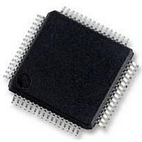
S9S12HY64J0MLH Freescale Semiconductor, S9S12HY64J0MLH Datasheet - Page 298

S9S12HY64J0MLH
Manufacturer Part Number
S9S12HY64J0MLH
Description
MCU 64K FLASH AUTO 64-LQFP
Manufacturer
Freescale Semiconductor
Series
HCS12r
Datasheet
1.S9S12HA32J0CLL.pdf
(792 pages)
Specifications of S9S12HY64J0MLH
Core Processor
HCS12
Core Size
16-Bit
Speed
32MHz
Connectivity
CAN, EBI/EMI, I²C, IrDA, LIN, SCI, SPI
Peripherals
LCD, Motor control PWM, POR, PWM, WDT
Number Of I /o
50
Program Memory Size
64KB (64K x 8)
Program Memory Type
FLASH
Eeprom Size
4K x 8
Ram Size
4K x 8
Voltage - Supply (vcc/vdd)
4.5 V ~ 5.5 V
Data Converters
A/D 6x10b
Oscillator Type
Internal
Operating Temperature
-40°C ~ 125°C
Package / Case
64-LQFP
Controller Family/series
S12
No. Of I/o's
50
Ram Memory Size
4KB
Cpu Speed
64MHz
No. Of Timers
2
Rohs Compliant
Yes
Processor Series
S12HY
Core
HCS12
3rd Party Development Tools
EWHCS12
Development Tools By Supplier
DEMO9S12HY64
Lead Free Status / RoHS Status
Lead free / RoHS Compliant
Available stocks
Company
Part Number
Manufacturer
Quantity
Price
Company:
Part Number:
S9S12HY64J0MLH
Manufacturer:
Freescale Semiconductor
Quantity:
10 000
- Current page: 298 of 792
- Download datasheet (4Mb)
Analog-to-Digital Converter (ADC12B8CV1) Block Description
8.3.2.8
Writes to this register will abort current conversion sequence.
Read: Anytime
Write: Anytime
298
Module Base + 0x0008
CMPE[7:0]
CC[3:0]
Reset
Field
Field
3–0
7–0
W
R
15
0
0
Conversion Counter — These 4 read-only bits are the binary value of the conversion counter. The conversion
counter points to the result register that will receive the result of the current conversion. E.g. CC3=0, CC2=1,
CC1=1, CC0=0 indicates that the result of the current conversion will be in ATD Result Register 6. If in non-FIFO
mode (FIFO=0) the conversion counter is initialized to zero at the begin and end of the conversion sequence. If
in FIFO mode (FIFO=1) the register counter is not initialized. The conversion counters wraps around when its
maximum value is reached.
Aborting a conversion or starting a new conversion clears the conversion counter even if FIFO=1.
Compare Enable for Conversion Number n (n= 7, 6, 5, 4, 3, 2, 1, 0) of a Sequence (n conversion number,
NOT channel number!) — These bits enable automatic compare of conversion results individually for
conversions of a sequence. The sense of each comparison is determined by the CMPHT[n] bit in the ATDCMPHT
register.
For each conversion number with CMPE[n]=1 do the following:
CCF[n] in ATDSTAT2 register will flag individual success of any comparison.
0 No automatic compare
1 Automatic compare of results for conversion n of a sequence is enabled.
ATD Compare Enable Register (ATDCMPE)
= Unimplemented or Reserved
1) Write compare value to ATDDRn result register
2) Write compare operator with CMPHT[n] in ATDCPMHT register
14
0
0
13
0
0
Figure 8-10. ATD Compare Enable Register (ATDCMPE)
Table 8-16. ATDSTAT0 Field Descriptions (continued)
12
0
0
MC9S12HY/HA-Family Reference Manual, Rev. 1.04
Table 8-17. ATDCMPE Field Descriptions
11
0
0
10
0
0
0
0
9
0
0
8
Description
Description
0
7
0
6
0
5
CMPE[7:0]
4
0
0
3
Freescale Semiconductor
0
2
0
1
0
0
Related parts for S9S12HY64J0MLH
Image
Part Number
Description
Manufacturer
Datasheet
Request
R
Part Number:
Description:
Manufacturer:
Freescale Semiconductor, Inc
Datasheet:
Part Number:
Description:
Manufacturer:
Freescale Semiconductor, Inc
Datasheet:
Part Number:
Description:
Manufacturer:
Freescale Semiconductor, Inc
Datasheet:
Part Number:
Description:
Manufacturer:
Freescale Semiconductor, Inc
Datasheet:
Part Number:
Description:
Manufacturer:
Freescale Semiconductor, Inc
Datasheet:
Part Number:
Description:
Manufacturer:
Freescale Semiconductor, Inc
Datasheet:
Part Number:
Description:
Manufacturer:
Freescale Semiconductor, Inc
Datasheet:
Part Number:
Description:
Manufacturer:
Freescale Semiconductor, Inc
Datasheet:
Part Number:
Description:
Manufacturer:
Freescale Semiconductor, Inc
Datasheet:
Part Number:
Description:
Manufacturer:
Freescale Semiconductor, Inc
Datasheet:
Part Number:
Description:
Manufacturer:
Freescale Semiconductor, Inc
Datasheet:
Part Number:
Description:
Manufacturer:
Freescale Semiconductor, Inc
Datasheet:
Part Number:
Description:
Manufacturer:
Freescale Semiconductor, Inc
Datasheet:
Part Number:
Description:
Manufacturer:
Freescale Semiconductor, Inc
Datasheet:
Part Number:
Description:
Manufacturer:
Freescale Semiconductor, Inc
Datasheet:


