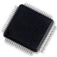
S9S12HY64J0MLH Freescale Semiconductor, S9S12HY64J0MLH Datasheet - Page 377

S9S12HY64J0MLH
Manufacturer Part Number
S9S12HY64J0MLH
Description
MCU 64K FLASH AUTO 64-LQFP
Manufacturer
Freescale Semiconductor
Series
HCS12r
Datasheet
1.S9S12HA32J0CLL.pdf
(792 pages)
Specifications of S9S12HY64J0MLH
Core Processor
HCS12
Core Size
16-Bit
Speed
32MHz
Connectivity
CAN, EBI/EMI, I²C, IrDA, LIN, SCI, SPI
Peripherals
LCD, Motor control PWM, POR, PWM, WDT
Number Of I /o
50
Program Memory Size
64KB (64K x 8)
Program Memory Type
FLASH
Eeprom Size
4K x 8
Ram Size
4K x 8
Voltage - Supply (vcc/vdd)
4.5 V ~ 5.5 V
Data Converters
A/D 6x10b
Oscillator Type
Internal
Operating Temperature
-40°C ~ 125°C
Package / Case
64-LQFP
Controller Family/series
S12
No. Of I/o's
50
Ram Memory Size
4KB
Cpu Speed
64MHz
No. Of Timers
2
Rohs Compliant
Yes
Processor Series
S12HY
Core
HCS12
3rd Party Development Tools
EWHCS12
Development Tools By Supplier
DEMO9S12HY64
Lead Free Status / RoHS Status
Lead free / RoHS Compliant
Available stocks
Company
Part Number
Manufacturer
Quantity
Price
Company:
Part Number:
S9S12HY64J0MLH
Manufacturer:
Freescale Semiconductor
Quantity:
10 000
- Current page: 377 of 792
- Download datasheet (4Mb)
DA
CL
DA
CL
Signal
10.4.1.1
When the bus is free, i.e. no master device is engaging the bus (both SCL and SDA lines are at logical
high), a master may initiate communication by sending a START signal.As shown in
START signal is defined as a high-to-low transition of SDA while SCL is high. This signal denotes the
beginning of a new data transfer (each data transfer may contain several bytes of data) and brings all slaves
out of their idle states.
Freescale Semiconductor
Signal
Start
Start
SCL
SDA
MSB
MSB
ADR7 ADR6 ADR5 ADR4ADR3 ADR2 ADR1R/W
ADR7 ADR6 ADR5 ADR4 ADR3 ADR2 ADR1R/W
1
1
2
2
START Signal
Calling Address
START Condition
Calling Address
3
3
4
4
5
5
MC9S12HY/HA-Family Reference Manual, Rev. 1.04
Figure 10-10. IIC-Bus Transmission Signals
Figure 10-11. Start and Stop Conditions
6
6
7
7
Read/
Write
Read/
Write
LSB
LSB
8
8
Ack
Ack
Bit
9
Bit
9
XX
Repeated
XXX
Signal
Start
MSB
MSB
ADR7 ADR6 ADR5 ADR4 ADR3 ADR2 ADR1R/W
D7
1
1
Inter-Integrated Circuit (IICV3) Block Description
D6
2
2
New Calling Address
D5
3
3
STOP Condition
Data Byte
D4
4
4
D3
5
5
Figure
D2
6
6
D1
7
7
10-10, a
Read/
Write
LSB
LSB
D0
8
8
Ack
No
Bit
Ack
9
No
9
Bit
377
Related parts for S9S12HY64J0MLH
Image
Part Number
Description
Manufacturer
Datasheet
Request
R
Part Number:
Description:
Manufacturer:
Freescale Semiconductor, Inc
Datasheet:
Part Number:
Description:
Manufacturer:
Freescale Semiconductor, Inc
Datasheet:
Part Number:
Description:
Manufacturer:
Freescale Semiconductor, Inc
Datasheet:
Part Number:
Description:
Manufacturer:
Freescale Semiconductor, Inc
Datasheet:
Part Number:
Description:
Manufacturer:
Freescale Semiconductor, Inc
Datasheet:
Part Number:
Description:
Manufacturer:
Freescale Semiconductor, Inc
Datasheet:
Part Number:
Description:
Manufacturer:
Freescale Semiconductor, Inc
Datasheet:
Part Number:
Description:
Manufacturer:
Freescale Semiconductor, Inc
Datasheet:
Part Number:
Description:
Manufacturer:
Freescale Semiconductor, Inc
Datasheet:
Part Number:
Description:
Manufacturer:
Freescale Semiconductor, Inc
Datasheet:
Part Number:
Description:
Manufacturer:
Freescale Semiconductor, Inc
Datasheet:
Part Number:
Description:
Manufacturer:
Freescale Semiconductor, Inc
Datasheet:
Part Number:
Description:
Manufacturer:
Freescale Semiconductor, Inc
Datasheet:
Part Number:
Description:
Manufacturer:
Freescale Semiconductor, Inc
Datasheet:
Part Number:
Description:
Manufacturer:
Freescale Semiconductor, Inc
Datasheet:


