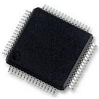
S9S12HY64J0MLH Freescale Semiconductor, S9S12HY64J0MLH Datasheet - Page 604

S9S12HY64J0MLH
Manufacturer Part Number
S9S12HY64J0MLH
Description
MCU 64K FLASH AUTO 64-LQFP
Manufacturer
Freescale Semiconductor
Series
HCS12r
Datasheet
1.S9S12HA32J0CLL.pdf
(792 pages)
Specifications of S9S12HY64J0MLH
Core Processor
HCS12
Core Size
16-Bit
Speed
32MHz
Connectivity
CAN, EBI/EMI, I²C, IrDA, LIN, SCI, SPI
Peripherals
LCD, Motor control PWM, POR, PWM, WDT
Number Of I /o
50
Program Memory Size
64KB (64K x 8)
Program Memory Type
FLASH
Eeprom Size
4K x 8
Ram Size
4K x 8
Voltage - Supply (vcc/vdd)
4.5 V ~ 5.5 V
Data Converters
A/D 6x10b
Oscillator Type
Internal
Operating Temperature
-40°C ~ 125°C
Package / Case
64-LQFP
Controller Family/series
S12
No. Of I/o's
50
Ram Memory Size
4KB
Cpu Speed
64MHz
No. Of Timers
2
Rohs Compliant
Yes
Processor Series
S12HY
Core
HCS12
3rd Party Development Tools
EWHCS12
Development Tools By Supplier
DEMO9S12HY64
Lead Free Status / RoHS Status
Lead free / RoHS Compliant
Available stocks
Company
Part Number
Manufacturer
Quantity
Price
Company:
Part Number:
S9S12HY64J0MLH
Manufacturer:
Freescale Semiconductor
Quantity:
10 000
- Current page: 604 of 792
- Download datasheet (4Mb)
48 KByte Flash Module (S12FTMRC48K1V1)
16.4.5.13 Set Field Margin Level Command
The Set Field Margin Level command, valid in special modes only, causes the Memory Controller to set
the margin level specified for future read operations of the P-Flash or D-Flash block.
Upon clearing CCIF to launch the Set Field Margin Level command, the Memory Controller will set the
field margin level for the targeted block and then set the CCIF flag.
Valid margin level settings for the Set Field Margin Level command are defined in
604
1
As defined by the memory map for FTMRC64K1.
Register
FSTAT
User margin levels can be used to check that Flash memory contents have
adequate margin for normal level read operations. If unexpected results are
encountered when checking Flash memory contents at user margin levels, a
potential loss of information has been detected.
CCOBIX[2:0]
When the D-Flash block is targeted, the D-Flash field margin levels are
applied only to the D-Flash reads. However, when the P-Flash block is
targeted, the P-Flash field margin levels are applied to both P-Flash and
D-Flash reads. It is not possible to apply field margin levels to the P-Flash
block only.
Table 16-56. Set Field Margin Level Command FCCOB Requirements
000
001
MGSTAT1
MGSTAT0
ACCERR
Table 16-55. Set User Margin Level Command Error Handling
Error Bit
FPVIOL
MC9S12HY/HA-Family Reference Manual, Rev. 1.04
Set if CCOBIX[2:0] != 001 at command launch
Set if command not available in current mode (see
Set if an invalid global address [17:16] is supplied
Set if an invalid margin level setting is supplied
None
None
None
0x0E
NOTE
NOTE
FCCOB Parameters
Margin level setting
Global address [17:16] to identify the Flash
Error Condition
block
1
Table
16-27)
Table
Freescale Semiconductor
16-57.
Related parts for S9S12HY64J0MLH
Image
Part Number
Description
Manufacturer
Datasheet
Request
R
Part Number:
Description:
Manufacturer:
Freescale Semiconductor, Inc
Datasheet:
Part Number:
Description:
Manufacturer:
Freescale Semiconductor, Inc
Datasheet:
Part Number:
Description:
Manufacturer:
Freescale Semiconductor, Inc
Datasheet:
Part Number:
Description:
Manufacturer:
Freescale Semiconductor, Inc
Datasheet:
Part Number:
Description:
Manufacturer:
Freescale Semiconductor, Inc
Datasheet:
Part Number:
Description:
Manufacturer:
Freescale Semiconductor, Inc
Datasheet:
Part Number:
Description:
Manufacturer:
Freescale Semiconductor, Inc
Datasheet:
Part Number:
Description:
Manufacturer:
Freescale Semiconductor, Inc
Datasheet:
Part Number:
Description:
Manufacturer:
Freescale Semiconductor, Inc
Datasheet:
Part Number:
Description:
Manufacturer:
Freescale Semiconductor, Inc
Datasheet:
Part Number:
Description:
Manufacturer:
Freescale Semiconductor, Inc
Datasheet:
Part Number:
Description:
Manufacturer:
Freescale Semiconductor, Inc
Datasheet:
Part Number:
Description:
Manufacturer:
Freescale Semiconductor, Inc
Datasheet:
Part Number:
Description:
Manufacturer:
Freescale Semiconductor, Inc
Datasheet:
Part Number:
Description:
Manufacturer:
Freescale Semiconductor, Inc
Datasheet:


