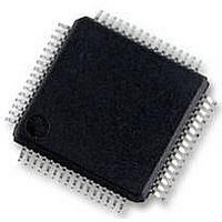
S9S12HY64J0MLH Freescale Semiconductor, S9S12HY64J0MLH Datasheet - Page 396

S9S12HY64J0MLH
Manufacturer Part Number
S9S12HY64J0MLH
Description
MCU 64K FLASH AUTO 64-LQFP
Manufacturer
Freescale Semiconductor
Series
HCS12r
Datasheet
1.S9S12HA32J0CLL.pdf
(792 pages)
Specifications of S9S12HY64J0MLH
Core Processor
HCS12
Core Size
16-Bit
Speed
32MHz
Connectivity
CAN, EBI/EMI, I²C, IrDA, LIN, SCI, SPI
Peripherals
LCD, Motor control PWM, POR, PWM, WDT
Number Of I /o
50
Program Memory Size
64KB (64K x 8)
Program Memory Type
FLASH
Eeprom Size
4K x 8
Ram Size
4K x 8
Voltage - Supply (vcc/vdd)
4.5 V ~ 5.5 V
Data Converters
A/D 6x10b
Oscillator Type
Internal
Operating Temperature
-40°C ~ 125°C
Package / Case
64-LQFP
Controller Family/series
S12
No. Of I/o's
50
Ram Memory Size
4KB
Cpu Speed
64MHz
No. Of Timers
2
Rohs Compliant
Yes
Processor Series
S12HY
Core
HCS12
3rd Party Development Tools
EWHCS12
Development Tools By Supplier
DEMO9S12HY64
Lead Free Status / RoHS Status
Lead free / RoHS Compliant
Available stocks
Company
Part Number
Manufacturer
Quantity
Price
Company:
Part Number:
S9S12HY64J0MLH
Manufacturer:
Freescale Semiconductor
Quantity:
10 000
- Current page: 396 of 792
- Download datasheet (4Mb)
Pulse-Width Modulator (S12PWM8B8CV1)
11.3.2.2
The starting polarity of each PWM channel waveform is determined by the associated PPOLx bit in the
PWMPOL register. If the polarity bit is one, the PWM channel output is high at the beginning of the cycle
and then goes low when the duty count is reached. Conversely, if the polarity bit is zero, the output starts
low and then goes high when the duty count is reached.
Read: Anytime
Write: Anytime
11.3.2.3
Each PWM channel has a choice of two clocks to use as the clock source for that channel as described
below.
396
Module Base + 0x0001
PPOL[7:0]
PWME1
PWME0
Reset
Field
Field
7–0
1
0
W
R
PPOL7
Pulse Width Channel 1 Enable
0 Pulse width channel 1 is disabled.
1 Pulse width channel 1 is enabled. The pulse modulated signal becomes available at PWM, output bit 1 when
Pulse Width Channel 0 Enable
0 Pulse width channel 0 is disabled.
1 Pulse width channel 0 is enabled. The pulse modulated signal becomes available at PWM, output bit 0 when
Pulse Width Channel 7–0 Polarity Bits
0 PWM channel 7–0 outputs are low at the beginning of the period, then go high when the duty count is
1 PWM channel 7–0 outputs are high at the beginning of the period, then go low when the duty count is
PWM Polarity Register (PWMPOL)
PWM Clock Select Register (PWMCLK)
0
7
PPOLx register bits can be written anytime. If the polarity is changed while
a PWM signal is being generated, a truncated or stretched pulse can occur
during the transition
its clock source begins its next cycle. If CON01 = 1, then bit has no effect and PWM output line0 is disabled.
reached.
reached.
its clock source begins its next cycle.
PPOL6
0
6
Table 11-1. PWME Field Descriptions (continued)
Figure 11-4. PWM Polarity Register (PWMPOL)
MC9S12HY/HA-Family Reference Manual, Rev. 1.04
Table 11-2. PWMPOL Field Descriptions
PPOL5
0
5
PPOL4
NOTE
0
4
Description
Description
PPOL3
0
3
PPOL2
0
2
PPOL1
Freescale Semiconductor
0
1
PPOL0
0
0
Related parts for S9S12HY64J0MLH
Image
Part Number
Description
Manufacturer
Datasheet
Request
R
Part Number:
Description:
Manufacturer:
Freescale Semiconductor, Inc
Datasheet:
Part Number:
Description:
Manufacturer:
Freescale Semiconductor, Inc
Datasheet:
Part Number:
Description:
Manufacturer:
Freescale Semiconductor, Inc
Datasheet:
Part Number:
Description:
Manufacturer:
Freescale Semiconductor, Inc
Datasheet:
Part Number:
Description:
Manufacturer:
Freescale Semiconductor, Inc
Datasheet:
Part Number:
Description:
Manufacturer:
Freescale Semiconductor, Inc
Datasheet:
Part Number:
Description:
Manufacturer:
Freescale Semiconductor, Inc
Datasheet:
Part Number:
Description:
Manufacturer:
Freescale Semiconductor, Inc
Datasheet:
Part Number:
Description:
Manufacturer:
Freescale Semiconductor, Inc
Datasheet:
Part Number:
Description:
Manufacturer:
Freescale Semiconductor, Inc
Datasheet:
Part Number:
Description:
Manufacturer:
Freescale Semiconductor, Inc
Datasheet:
Part Number:
Description:
Manufacturer:
Freescale Semiconductor, Inc
Datasheet:
Part Number:
Description:
Manufacturer:
Freescale Semiconductor, Inc
Datasheet:
Part Number:
Description:
Manufacturer:
Freescale Semiconductor, Inc
Datasheet:
Part Number:
Description:
Manufacturer:
Freescale Semiconductor, Inc
Datasheet:


