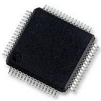
S9S12HY64J0MLH Freescale Semiconductor, S9S12HY64J0MLH Datasheet - Page 381

S9S12HY64J0MLH
Manufacturer Part Number
S9S12HY64J0MLH
Description
MCU 64K FLASH AUTO 64-LQFP
Manufacturer
Freescale Semiconductor
Series
HCS12r
Datasheet
1.S9S12HA32J0CLL.pdf
(792 pages)
Specifications of S9S12HY64J0MLH
Core Processor
HCS12
Core Size
16-Bit
Speed
32MHz
Connectivity
CAN, EBI/EMI, I²C, IrDA, LIN, SCI, SPI
Peripherals
LCD, Motor control PWM, POR, PWM, WDT
Number Of I /o
50
Program Memory Size
64KB (64K x 8)
Program Memory Type
FLASH
Eeprom Size
4K x 8
Ram Size
4K x 8
Voltage - Supply (vcc/vdd)
4.5 V ~ 5.5 V
Data Converters
A/D 6x10b
Oscillator Type
Internal
Operating Temperature
-40°C ~ 125°C
Package / Case
64-LQFP
Controller Family/series
S12
No. Of I/o's
50
Ram Memory Size
4KB
Cpu Speed
64MHz
No. Of Timers
2
Rohs Compliant
Yes
Processor Series
S12HY
Core
HCS12
3rd Party Development Tools
EWHCS12
Development Tools By Supplier
DEMO9S12HY64
Lead Free Status / RoHS Status
Lead free / RoHS Compliant
Available stocks
Company
Part Number
Manufacturer
Quantity
Price
Company:
Part Number:
S9S12HY64J0MLH
Manufacturer:
Freescale Semiconductor
Quantity:
10 000
- Current page: 381 of 792
- Download datasheet (4Mb)
10.4.1.11 General Call Address
To broadcast using a general call, a device must first generate the general call address($00), then after
receiving acknowledge, it must transmit data.
In communication, as a slave device, provided the GCEN is asserted, a device acknowledges the broadcast
and receives data until the GCEN is disabled or the master device releases the bus or generates a new
transfer. In the broadcast, slaves always act as receivers. In general call, IAAS is also used to indicate the
address match.
In order to distinguish whether the address match is the normal address match or the general call address
match, IBDR should be read after the address byte has been received. If the data is $00, the match is
general call address match. The meaning of the general call address is always specified in the first data byte
and must be dealt with by S/W, the IIC hardware does not decode and process the first data byte.
When one byte transfer is done, the received data can be read from IBDR. The user can control the
procedure by enabling or disabling GCEN.
10.4.2
This is the basic mode of operation.
10.4.3
IIC operation in wait mode can be configured. Depending on the state of internal bits, the IIC can operate
normally when the CPU is in wait mode or the IIC clock generation can be turned off and the IIC module
enters a power conservation state during wait mode. In the later case, any transmission or reception in
progress stops at wait mode entry.
10.4.4
The IIC is inactive in stop mode for reduced power consumption. The STOP instruction does not affect IIC
register states.
10.5
The reset state of each individual bit is listed in
which details the registers and their bit-fields.
10.6
IICV3 uses only one interrupt vector.
Freescale Semiconductor
Interrupt
Resets
Interrupts
Operation in Run Mode
Operation in Wait Mode
Operation in Stop Mode
Offset
Vector
MC9S12HY/HA-Family Reference Manual, Rev. 1.04
Priority
Table 10-11. Interrupt Summary
Section 10.3, “Memory Map and Register
Source
Inter-Integrated Circuit (IICV3) Block Description
Description
Definition,”
381
Related parts for S9S12HY64J0MLH
Image
Part Number
Description
Manufacturer
Datasheet
Request
R
Part Number:
Description:
Manufacturer:
Freescale Semiconductor, Inc
Datasheet:
Part Number:
Description:
Manufacturer:
Freescale Semiconductor, Inc
Datasheet:
Part Number:
Description:
Manufacturer:
Freescale Semiconductor, Inc
Datasheet:
Part Number:
Description:
Manufacturer:
Freescale Semiconductor, Inc
Datasheet:
Part Number:
Description:
Manufacturer:
Freescale Semiconductor, Inc
Datasheet:
Part Number:
Description:
Manufacturer:
Freescale Semiconductor, Inc
Datasheet:
Part Number:
Description:
Manufacturer:
Freescale Semiconductor, Inc
Datasheet:
Part Number:
Description:
Manufacturer:
Freescale Semiconductor, Inc
Datasheet:
Part Number:
Description:
Manufacturer:
Freescale Semiconductor, Inc
Datasheet:
Part Number:
Description:
Manufacturer:
Freescale Semiconductor, Inc
Datasheet:
Part Number:
Description:
Manufacturer:
Freescale Semiconductor, Inc
Datasheet:
Part Number:
Description:
Manufacturer:
Freescale Semiconductor, Inc
Datasheet:
Part Number:
Description:
Manufacturer:
Freescale Semiconductor, Inc
Datasheet:
Part Number:
Description:
Manufacturer:
Freescale Semiconductor, Inc
Datasheet:
Part Number:
Description:
Manufacturer:
Freescale Semiconductor, Inc
Datasheet:


