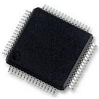
S9S12HY64J0MLH Freescale Semiconductor, S9S12HY64J0MLH Datasheet - Page 81

S9S12HY64J0MLH
Manufacturer Part Number
S9S12HY64J0MLH
Description
MCU 64K FLASH AUTO 64-LQFP
Manufacturer
Freescale Semiconductor
Series
HCS12r
Datasheet
1.S9S12HA32J0CLL.pdf
(792 pages)
Specifications of S9S12HY64J0MLH
Core Processor
HCS12
Core Size
16-Bit
Speed
32MHz
Connectivity
CAN, EBI/EMI, I²C, IrDA, LIN, SCI, SPI
Peripherals
LCD, Motor control PWM, POR, PWM, WDT
Number Of I /o
50
Program Memory Size
64KB (64K x 8)
Program Memory Type
FLASH
Eeprom Size
4K x 8
Ram Size
4K x 8
Voltage - Supply (vcc/vdd)
4.5 V ~ 5.5 V
Data Converters
A/D 6x10b
Oscillator Type
Internal
Operating Temperature
-40°C ~ 125°C
Package / Case
64-LQFP
Controller Family/series
S12
No. Of I/o's
50
Ram Memory Size
4KB
Cpu Speed
64MHz
No. Of Timers
2
Rohs Compliant
Yes
Processor Series
S12HY
Core
HCS12
3rd Party Development Tools
EWHCS12
Development Tools By Supplier
DEMO9S12HY64
Lead Free Status / RoHS Status
Lead free / RoHS Compliant
Available stocks
Company
Part Number
Manufacturer
Quantity
Price
Company:
Part Number:
S9S12HY64J0MLH
Manufacturer:
Freescale Semiconductor
Quantity:
10 000
- Current page: 81 of 792
- Download datasheet (4Mb)
1
2.3.16
2.3.17
Freescale Semiconductor
Address 0x0242
Address 0x0243
Read: Anytime
Write: Anytime
DDRT
DDRT
Field
Reset
Reset
7-4
3-0
W
W
R
R
Port T data direction—
This bit determines whether the pin is an input or output.
If corresponding LCD segment is enabled, it will be forced as input/output disabled
Else If corresponding TIM0 output compare channel is enabled, it will be forced as output.
1 Associated pin is configured as output
0 Associated pin is configured as input
Port T data direction—
This bit determines whether the pin is an input or output.
If corresponding LCD segment is enabled, it will be forced as input/output disabled
Else If corresponding TIM1 output compare channel is enabled, it will be forced as output.
1 Associated pin is configured as output
0 Associated pin is configured as input
DDRT7
RDRT7
Port T Data Direction Register (DDRT)
Port T Reduced Drive Register (RDRT)
0
0
7
7
Due to internal synchronization circuits, it can take up to 2 bus clock cycles
until the correct value is read on PTT or PTIT registers, when changing the
DDRT register.
DDRT6
RDRT6
0
0
6
6
Figure 2-15. Port T Reduced Drive Register (RDRT)
Figure 2-14. Port T Data Direction Register (DDRT)
MC9S12HY/HA-Family Reference Manual, Rev. 1.04
Table 2-14. DDRT Register Field Descriptions
DDRT5
RDRT5
0
0
5
5
DDRT4
RDRT4
NOTE
0
0
4
4
Description
DDRT3
RDRT3
3
0
3
0
RDRT2
DDRT2
Port Integration Module (S12HYPIMV1)
0
0
2
2
DDRT1
RDRT1
Access: User read/write
Access: User read/write
0
0
1
1
DDRT0
RDRT0
0
0
0
0
81
1
1
Related parts for S9S12HY64J0MLH
Image
Part Number
Description
Manufacturer
Datasheet
Request
R
Part Number:
Description:
Manufacturer:
Freescale Semiconductor, Inc
Datasheet:
Part Number:
Description:
Manufacturer:
Freescale Semiconductor, Inc
Datasheet:
Part Number:
Description:
Manufacturer:
Freescale Semiconductor, Inc
Datasheet:
Part Number:
Description:
Manufacturer:
Freescale Semiconductor, Inc
Datasheet:
Part Number:
Description:
Manufacturer:
Freescale Semiconductor, Inc
Datasheet:
Part Number:
Description:
Manufacturer:
Freescale Semiconductor, Inc
Datasheet:
Part Number:
Description:
Manufacturer:
Freescale Semiconductor, Inc
Datasheet:
Part Number:
Description:
Manufacturer:
Freescale Semiconductor, Inc
Datasheet:
Part Number:
Description:
Manufacturer:
Freescale Semiconductor, Inc
Datasheet:
Part Number:
Description:
Manufacturer:
Freescale Semiconductor, Inc
Datasheet:
Part Number:
Description:
Manufacturer:
Freescale Semiconductor, Inc
Datasheet:
Part Number:
Description:
Manufacturer:
Freescale Semiconductor, Inc
Datasheet:
Part Number:
Description:
Manufacturer:
Freescale Semiconductor, Inc
Datasheet:
Part Number:
Description:
Manufacturer:
Freescale Semiconductor, Inc
Datasheet:
Part Number:
Description:
Manufacturer:
Freescale Semiconductor, Inc
Datasheet:


