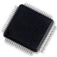
S9S12HY64J0MLH Freescale Semiconductor, S9S12HY64J0MLH Datasheet - Page 674

S9S12HY64J0MLH
Manufacturer Part Number
S9S12HY64J0MLH
Description
MCU 64K FLASH AUTO 64-LQFP
Manufacturer
Freescale Semiconductor
Series
HCS12r
Datasheet
1.S9S12HA32J0CLL.pdf
(792 pages)
Specifications of S9S12HY64J0MLH
Core Processor
HCS12
Core Size
16-Bit
Speed
32MHz
Connectivity
CAN, EBI/EMI, I²C, IrDA, LIN, SCI, SPI
Peripherals
LCD, Motor control PWM, POR, PWM, WDT
Number Of I /o
50
Program Memory Size
64KB (64K x 8)
Program Memory Type
FLASH
Eeprom Size
4K x 8
Ram Size
4K x 8
Voltage - Supply (vcc/vdd)
4.5 V ~ 5.5 V
Data Converters
A/D 6x10b
Oscillator Type
Internal
Operating Temperature
-40°C ~ 125°C
Package / Case
64-LQFP
Controller Family/series
S12
No. Of I/o's
50
Ram Memory Size
4KB
Cpu Speed
64MHz
No. Of Timers
2
Rohs Compliant
Yes
Processor Series
S12HY
Core
HCS12
3rd Party Development Tools
EWHCS12
Development Tools By Supplier
DEMO9S12HY64
Lead Free Status / RoHS Status
Lead free / RoHS Compliant
Available stocks
Company
Part Number
Manufacturer
Quantity
Price
Company:
Part Number:
S9S12HY64J0MLH
Manufacturer:
Freescale Semiconductor
Quantity:
10 000
- Current page: 674 of 792
- Download datasheet (4Mb)
Liquid Crystal Display (LCD40F4BV1) Block Description
For other combinations of IRCCLK and divider not shown in
used to calculate the LCD frame frequency for each multiplex mode:
The possible divider values are shown in
18.4.1.3
For a segment on the LCD to be displayed, data must be written to the LCD RAM which is shown in
Section 18.3, “Memory Map and Register
160 segments that are driven by the frontplane and backplane drivers. Writing a 1 to a given location will
result in the corresponding display segment being driven with a differential RMS voltage necessary to turn
the segment ON when the LCDEN bit is set and the corresponding FP[39:0]EN bit is set. Writing a 0 to a
given location will result in the corresponding display segment being driven with a differential RMS
voltage necessary to turn the segment OFF. The LCD RAM is a dual port RAM that interfaces with the
internal address and data buses of the MCU. It is possible to read from LCD RAM locations for scrolling
purposes. When LCDEN = 0, the LCD RAM can be used as on-chip RAM. Writing or reading of the
LCDEN bit does not change the contents of the LCD RAM. After a reset, the LCD RAM contents will be
indeterminate.
18.4.1.4
If LCDEN = 0 (LCD40F4BV1 driver system disabled) and the frontplane enable bit, FP[39:0]EN, is set,
the frontplane driver waveform will not appear on the output until LCDEN is set. If LCDEN = 1
(LCD40F4BV1 driver system enabled), the frontplane driver waveform will appear on the output as soon
as the corresponding frontplane enable bit, FP[39:0]EN, in the registers FPENR0–FPENR4 is set.
18.4.1.5
The LCD40F4BV1 driver has five modes of operation:
674
IRCCLK = 16.0
Source clock
Frequency in
•
•
•
•
•
MHz
1/1 duty (1 backplane), 1/1 bias (2 voltage levels)
1/2 duty (2 backplanes), 1/2 bias (3 voltage levels)
1/2 duty (2 backplanes), 1/3 bias (4 voltage levels)
1/3 duty (3 backplanes), 1/3 bias (4 voltage levels)
1/4 duty (4 backplanes), 1/3 bias (4 voltage levels)
LCD RAM
LCD Driver System Enable and Frontplane Enable Sequencing
LCD Bias and Modes of Operation
LCLK2
LCD Clock Prescaler
1
1
LCD Frame Frequency (Hz)
LCLK1
1
1
MC9S12HY/HA-Family Reference Manual, Rev. 1.04
Table 18-8. LCD Clock and Frame Frequency
LCLK0
0
1
Table
Definition”. The 160 bits in the LCD RAM correspond to the
Divider
131072
65536
18-8.
Frequency [Hz]
=
LCD Clock
244
122
-------------------------------------- -
IRCCLK (Hz)
Divider
Table
1/1 Duty
18-8, the following formula may be
244
122
Frame Frequency [Hz]
Duty
1/2 Duty
122
61
Freescale Semiconductor
1/3 Duty
81
40
1/4 Duty
61
31
Related parts for S9S12HY64J0MLH
Image
Part Number
Description
Manufacturer
Datasheet
Request
R
Part Number:
Description:
Manufacturer:
Freescale Semiconductor, Inc
Datasheet:
Part Number:
Description:
Manufacturer:
Freescale Semiconductor, Inc
Datasheet:
Part Number:
Description:
Manufacturer:
Freescale Semiconductor, Inc
Datasheet:
Part Number:
Description:
Manufacturer:
Freescale Semiconductor, Inc
Datasheet:
Part Number:
Description:
Manufacturer:
Freescale Semiconductor, Inc
Datasheet:
Part Number:
Description:
Manufacturer:
Freescale Semiconductor, Inc
Datasheet:
Part Number:
Description:
Manufacturer:
Freescale Semiconductor, Inc
Datasheet:
Part Number:
Description:
Manufacturer:
Freescale Semiconductor, Inc
Datasheet:
Part Number:
Description:
Manufacturer:
Freescale Semiconductor, Inc
Datasheet:
Part Number:
Description:
Manufacturer:
Freescale Semiconductor, Inc
Datasheet:
Part Number:
Description:
Manufacturer:
Freescale Semiconductor, Inc
Datasheet:
Part Number:
Description:
Manufacturer:
Freescale Semiconductor, Inc
Datasheet:
Part Number:
Description:
Manufacturer:
Freescale Semiconductor, Inc
Datasheet:
Part Number:
Description:
Manufacturer:
Freescale Semiconductor, Inc
Datasheet:
Part Number:
Description:
Manufacturer:
Freescale Semiconductor, Inc
Datasheet:


