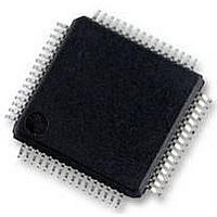
S9S12HY64J0MLH Freescale Semiconductor, S9S12HY64J0MLH Datasheet - Page 219

S9S12HY64J0MLH
Manufacturer Part Number
S9S12HY64J0MLH
Description
MCU 64K FLASH AUTO 64-LQFP
Manufacturer
Freescale Semiconductor
Series
HCS12r
Datasheet
1.S9S12HA32J0CLL.pdf
(792 pages)
Specifications of S9S12HY64J0MLH
Core Processor
HCS12
Core Size
16-Bit
Speed
32MHz
Connectivity
CAN, EBI/EMI, I²C, IrDA, LIN, SCI, SPI
Peripherals
LCD, Motor control PWM, POR, PWM, WDT
Number Of I /o
50
Program Memory Size
64KB (64K x 8)
Program Memory Type
FLASH
Eeprom Size
4K x 8
Ram Size
4K x 8
Voltage - Supply (vcc/vdd)
4.5 V ~ 5.5 V
Data Converters
A/D 6x10b
Oscillator Type
Internal
Operating Temperature
-40°C ~ 125°C
Package / Case
64-LQFP
Controller Family/series
S12
No. Of I/o's
50
Ram Memory Size
4KB
Cpu Speed
64MHz
No. Of Timers
2
Rohs Compliant
Yes
Processor Series
S12HY
Core
HCS12
3rd Party Development Tools
EWHCS12
Development Tools By Supplier
DEMO9S12HY64
Lead Free Status / RoHS Status
Lead free / RoHS Compliant
Available stocks
Company
Part Number
Manufacturer
Quantity
Price
Company:
Part Number:
S9S12HY64J0MLH
Manufacturer:
Freescale Semiconductor
Quantity:
10 000
- Current page: 219 of 792
- Download datasheet (4Mb)
BDM cannot be entered from a breakpoint unless the ENABLE bit is set in the BDM. If entry to BDM via
a BGND instruction is attempted and the ENABLE bit in the BDM is cleared, the CPU actually executes
the BDM firmware code, checks the ENABLE and returns if ENABLE is not set. If not serviced by the
monitor then the breakpoint is re-asserted when the BDM returns to normal CPU flow.
If the comparator register contents coincide with the SWI/BDM vector address then an SWI in user code
could coincide with a DBG breakpoint. The CPU ensures that BDM requests have a higher priority than
SWI requests. Returning from the BDM/SWI service routine care must be taken to avoid a repeated
breakpoint at the same address.
Should a tagged or forced breakpoint coincide with a BGND in user code, then the instruction that follows
the BGND instruction is the first instruction executed when normal program execution resumes.
6.5
6.5.1
Defining the state control registers as SCR1,SCR2, SCR3 and M0,M1,M2 as matches on channels 0,1,2
respectively. SCR encoding supported by S12SDBGV1 are shown in black. SCR encoding supported only
in S12SDBGV2 are shown in red. For backwards compatibility the new scenarios use a 4th bit in each SCR
register. Thus the existing encoding for SCRx[2:0] is not changed.
Freescale Semiconductor
Application Information
DBGBRK
State Machine scenarios
0
1
X
1
1
When program control returns from a tagged breakpoint using an RTI or
BDM GO command without program counter modification it returns to the
instruction whose tag generated the breakpoint. To avoid a repeated
breakpoint at the same location reconfigure the DBG module in the SWI
routine, if configured for an SWI breakpoint, or over the BDM interface by
executing a TRACE command before the GO to increment the program flow
past the tagged instruction.
(DBGC1[4])
BDM Bit
MC9S12HY/HA-Family Reference Manual, Rev. 1.04
Table 6-43. Breakpoint Mapping Summary
X
X
0
1
1
Enabled
BDM
X
X
1
0
1
NOTE
Active
BDM
X
X
0
1
0
Breakpoint to BDM
Breakpoint to SWI
Breakpoint to SWI
S12S Debug Module (S12SDBGV2)
No Breakpoint
No Breakpoint
Breakpoint
Mapping
219
Related parts for S9S12HY64J0MLH
Image
Part Number
Description
Manufacturer
Datasheet
Request
R
Part Number:
Description:
Manufacturer:
Freescale Semiconductor, Inc
Datasheet:
Part Number:
Description:
Manufacturer:
Freescale Semiconductor, Inc
Datasheet:
Part Number:
Description:
Manufacturer:
Freescale Semiconductor, Inc
Datasheet:
Part Number:
Description:
Manufacturer:
Freescale Semiconductor, Inc
Datasheet:
Part Number:
Description:
Manufacturer:
Freescale Semiconductor, Inc
Datasheet:
Part Number:
Description:
Manufacturer:
Freescale Semiconductor, Inc
Datasheet:
Part Number:
Description:
Manufacturer:
Freescale Semiconductor, Inc
Datasheet:
Part Number:
Description:
Manufacturer:
Freescale Semiconductor, Inc
Datasheet:
Part Number:
Description:
Manufacturer:
Freescale Semiconductor, Inc
Datasheet:
Part Number:
Description:
Manufacturer:
Freescale Semiconductor, Inc
Datasheet:
Part Number:
Description:
Manufacturer:
Freescale Semiconductor, Inc
Datasheet:
Part Number:
Description:
Manufacturer:
Freescale Semiconductor, Inc
Datasheet:
Part Number:
Description:
Manufacturer:
Freescale Semiconductor, Inc
Datasheet:
Part Number:
Description:
Manufacturer:
Freescale Semiconductor, Inc
Datasheet:
Part Number:
Description:
Manufacturer:
Freescale Semiconductor, Inc
Datasheet:


