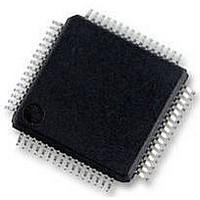
S9S12HY64J0MLH Freescale Semiconductor, S9S12HY64J0MLH Datasheet - Page 404

S9S12HY64J0MLH
Manufacturer Part Number
S9S12HY64J0MLH
Description
MCU 64K FLASH AUTO 64-LQFP
Manufacturer
Freescale Semiconductor
Series
HCS12r
Datasheet
1.S9S12HA32J0CLL.pdf
(792 pages)
Specifications of S9S12HY64J0MLH
Core Processor
HCS12
Core Size
16-Bit
Speed
32MHz
Connectivity
CAN, EBI/EMI, I²C, IrDA, LIN, SCI, SPI
Peripherals
LCD, Motor control PWM, POR, PWM, WDT
Number Of I /o
50
Program Memory Size
64KB (64K x 8)
Program Memory Type
FLASH
Eeprom Size
4K x 8
Ram Size
4K x 8
Voltage - Supply (vcc/vdd)
4.5 V ~ 5.5 V
Data Converters
A/D 6x10b
Oscillator Type
Internal
Operating Temperature
-40°C ~ 125°C
Package / Case
64-LQFP
Controller Family/series
S12
No. Of I/o's
50
Ram Memory Size
4KB
Cpu Speed
64MHz
No. Of Timers
2
Rohs Compliant
Yes
Processor Series
S12HY
Core
HCS12
3rd Party Development Tools
EWHCS12
Development Tools By Supplier
DEMO9S12HY64
Lead Free Status / RoHS Status
Lead free / RoHS Compliant
Available stocks
Company
Part Number
Manufacturer
Quantity
Price
Company:
Part Number:
S9S12HY64J0MLH
Manufacturer:
Freescale Semiconductor
Quantity:
10 000
- Current page: 404 of 792
- Download datasheet (4Mb)
Pulse-Width Modulator (S12PWM8B8CV1)
Write: Anytime (any value written causes PWM counter to be reset to $00).
11.3.2.13 PWM Channel Period Registers (PWMPERx)
There is a dedicated period register for each channel. The value in this register determines the period of
the associated PWM channel.
The period registers for each channel are double buffered so that if they change while the channel is
enabled, the change will NOT take effect until one of the following occurs:
In this way, the output of the PWM will always be either the old waveform or the new waveform, not some
variation in between. If the channel is not enabled, then writes to the period register will go directly to the
latches as well as the buffer.
See
To calculate the output period, take the selected clock source period for the channel of interest (A, B, SA,
or SB) and multiply it by the value in the period register for that channel:
For boundary case programming values, please refer to
Read: Anytime
Write: Anytime
404
Module Base + 0x0014 = PWMPER0, 0x0015 = PWMPER1, 0x0016 = PWMPER2, 0x0017 = PWMPER3
Module Base + 0x0018 = PWMPER4, 0x0019 = PWMPER5, 0x001A = PWMPER6, 0x001B = PWMPER7
Reset
•
•
•
•
•
Section 11.4.2.3, “PWM Period and Duty”
W
R
The effective period ends
The counter is written (counter resets to $00)
The channel is disabled
Left aligned output (CAEx = 0)
PWMx Period = Channel Clock Period * PWMPERx Center Aligned Output (CAEx = 1)
PWMx Period = Channel Clock Period * (2 * PWMPERx)
Bit 7
1
7
Reads of this register return the most recent value written. Reads do not
necessarily return the value of the currently active period due to the double
buffering scheme.
Figure 11-15. PWM Channel Period Registers (PWMPERx)
1
6
6
MC9S12HY/HA-Family Reference Manual, Rev. 1.04
1
5
5
for more information.
NOTE
1
4
4
Section 11.4.2.8, “PWM Boundary
1
3
3
1
2
2
Freescale Semiconductor
1
1
1
Cases”.
Bit 0
1
0
Related parts for S9S12HY64J0MLH
Image
Part Number
Description
Manufacturer
Datasheet
Request
R
Part Number:
Description:
Manufacturer:
Freescale Semiconductor, Inc
Datasheet:
Part Number:
Description:
Manufacturer:
Freescale Semiconductor, Inc
Datasheet:
Part Number:
Description:
Manufacturer:
Freescale Semiconductor, Inc
Datasheet:
Part Number:
Description:
Manufacturer:
Freescale Semiconductor, Inc
Datasheet:
Part Number:
Description:
Manufacturer:
Freescale Semiconductor, Inc
Datasheet:
Part Number:
Description:
Manufacturer:
Freescale Semiconductor, Inc
Datasheet:
Part Number:
Description:
Manufacturer:
Freescale Semiconductor, Inc
Datasheet:
Part Number:
Description:
Manufacturer:
Freescale Semiconductor, Inc
Datasheet:
Part Number:
Description:
Manufacturer:
Freescale Semiconductor, Inc
Datasheet:
Part Number:
Description:
Manufacturer:
Freescale Semiconductor, Inc
Datasheet:
Part Number:
Description:
Manufacturer:
Freescale Semiconductor, Inc
Datasheet:
Part Number:
Description:
Manufacturer:
Freescale Semiconductor, Inc
Datasheet:
Part Number:
Description:
Manufacturer:
Freescale Semiconductor, Inc
Datasheet:
Part Number:
Description:
Manufacturer:
Freescale Semiconductor, Inc
Datasheet:
Part Number:
Description:
Manufacturer:
Freescale Semiconductor, Inc
Datasheet:


