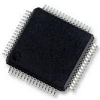
S9S12HY64J0MLH Freescale Semiconductor, S9S12HY64J0MLH Datasheet - Page 400

S9S12HY64J0MLH
Manufacturer Part Number
S9S12HY64J0MLH
Description
MCU 64K FLASH AUTO 64-LQFP
Manufacturer
Freescale Semiconductor
Series
HCS12r
Datasheet
1.S9S12HA32J0CLL.pdf
(792 pages)
Specifications of S9S12HY64J0MLH
Core Processor
HCS12
Core Size
16-Bit
Speed
32MHz
Connectivity
CAN, EBI/EMI, I²C, IrDA, LIN, SCI, SPI
Peripherals
LCD, Motor control PWM, POR, PWM, WDT
Number Of I /o
50
Program Memory Size
64KB (64K x 8)
Program Memory Type
FLASH
Eeprom Size
4K x 8
Ram Size
4K x 8
Voltage - Supply (vcc/vdd)
4.5 V ~ 5.5 V
Data Converters
A/D 6x10b
Oscillator Type
Internal
Operating Temperature
-40°C ~ 125°C
Package / Case
64-LQFP
Controller Family/series
S12
No. Of I/o's
50
Ram Memory Size
4KB
Cpu Speed
64MHz
No. Of Timers
2
Rohs Compliant
Yes
Processor Series
S12HY
Core
HCS12
3rd Party Development Tools
EWHCS12
Development Tools By Supplier
DEMO9S12HY64
Lead Free Status / RoHS Status
Lead free / RoHS Compliant
Available stocks
Company
Part Number
Manufacturer
Quantity
Price
Company:
Part Number:
S9S12HY64J0MLH
Manufacturer:
Freescale Semiconductor
Quantity:
10 000
- Current page: 400 of 792
- Download datasheet (4Mb)
Pulse-Width Modulator (S12PWM8B8CV1)
2 registers become the high order bytes of the double byte channel. When channels 0 and 1 are
concatenated, channel 0 registers become the high order bytes of the double byte channel.
See
Function.
400
CON67
CON45
CON23
CON01
PFREZ
PSWAI
Field
Section 11.4.2.7, “PWM 16-Bit Functions”
7
6
5
4
3
2
Concatenate Channels 6 and 7
0 Channels 6 and 7 are separate 8-bit PWMs.
1 Channels 6 and 7 are concatenated to create one 16-bit PWM channel. Channel 6 becomes the high order
Concatenate Channels 4 and 5
0 Channels 4 and 5 are separate 8-bit PWMs.
1 Channels 4 and 5 are concatenated to create one 16-bit PWM channel. Channel 4 becomes the high order
Concatenate Channels 2 and 3
0 Channels 2 and 3 are separate 8-bit PWMs.
1 Channels 2 and 3 are concatenated to create one 16-bit PWM channel. Channel 2 becomes the high order
Concatenate Channels 0 and 1
0 Channels 0 and 1 are separate 8-bit PWMs.
1 Channels 0 and 1 are concatenated to create one 16-bit PWM channel. Channel 0 becomes the high order
PWM Stops in Wait Mode — Enabling this bit allows for lower power consumption in wait mode by disabling
the input clock to the prescaler.
0 Allow the clock to the prescaler to continue while in wait mode.
1 Stop the input clock to the prescaler whenever the MCU is in wait mode.
PWM Counters Stop in Freeze Mode — In freeze mode, there is an option to disable the input clock to the
prescaler by setting the PFRZ bit in the PWMCTL register. If this bit is set, whenever the MCU is in freeze mode,
the input clock to the prescaler is disabled. This feature is useful during emulation as it allows the PWM function
to be suspended. In this way, the counters of the PWM can be stopped while in freeze mode so that once normal
program flow is continued, the counters are re-enabled to simulate real-time operations. Since the registers can
still be accessed in this mode, to re-enable the prescaler clock, either disable the PFRZ bit or exit freeze mode.
0 Allow PWM to continue while in freeze mode.
1 Disable PWM input clock to the prescaler whenever the part is in freeze mode. This is useful for emulation.
Change these bits only when both corresponding channels are disabled.
byte and channel 7 becomes the low order byte. Channel 7 output pin is used as the output for this 16-bit
PWM (bit 7 of port PWMP). Channel 7 clock select control-bit determines the clock source, channel 7 polarity
bit determines the polarity, channel 7 enable bit enables the output and channel 7 center aligned enable bit
determines the output mode.
byte and channel 5 becomes the low order byte. Channel 5 output pin is used as the output for this 16-bit
PWM (bit 5 of port PWMP). Channel 5 clock select control-bit determines the clock source, channel 5 polarity
bit determines the polarity, channel 5 enable bit enables the output and channel 5 center aligned enable bit
determines the output mode.
byte and channel 3 becomes the low order byte. Channel 3 output pin is used as the output for this 16-bit
PWM (bit 3 of port PWMP). Channel 3 clock select control-bit determines the clock source, channel 3 polarity
bit determines the polarity, channel 3 enable bit enables the output and channel 3 center aligned enable bit
determines the output mode.
byte and channel 1 becomes the low order byte. Channel 1 output pin is used as the output for this 16-bit
PWM (bit 1 of port PWMP). Channel 1 clock select control-bit determines the clock source, channel 1 polarity
bit determines the polarity, channel 1 enable bit enables the output and channel 1 center aligned enable bit
determines the output mode.
MC9S12HY/HA-Family Reference Manual, Rev. 1.04
Table 11-8. PWMCTL Field Descriptions
for a more detailed description of the concatenation PWM
NOTE
Description
Freescale Semiconductor
Related parts for S9S12HY64J0MLH
Image
Part Number
Description
Manufacturer
Datasheet
Request
R
Part Number:
Description:
Manufacturer:
Freescale Semiconductor, Inc
Datasheet:
Part Number:
Description:
Manufacturer:
Freescale Semiconductor, Inc
Datasheet:
Part Number:
Description:
Manufacturer:
Freescale Semiconductor, Inc
Datasheet:
Part Number:
Description:
Manufacturer:
Freescale Semiconductor, Inc
Datasheet:
Part Number:
Description:
Manufacturer:
Freescale Semiconductor, Inc
Datasheet:
Part Number:
Description:
Manufacturer:
Freescale Semiconductor, Inc
Datasheet:
Part Number:
Description:
Manufacturer:
Freescale Semiconductor, Inc
Datasheet:
Part Number:
Description:
Manufacturer:
Freescale Semiconductor, Inc
Datasheet:
Part Number:
Description:
Manufacturer:
Freescale Semiconductor, Inc
Datasheet:
Part Number:
Description:
Manufacturer:
Freescale Semiconductor, Inc
Datasheet:
Part Number:
Description:
Manufacturer:
Freescale Semiconductor, Inc
Datasheet:
Part Number:
Description:
Manufacturer:
Freescale Semiconductor, Inc
Datasheet:
Part Number:
Description:
Manufacturer:
Freescale Semiconductor, Inc
Datasheet:
Part Number:
Description:
Manufacturer:
Freescale Semiconductor, Inc
Datasheet:
Part Number:
Description:
Manufacturer:
Freescale Semiconductor, Inc
Datasheet:


