HD64F36912GFH Renesas Electronics America, HD64F36912GFH Datasheet - Page 22
HD64F36912GFH
Manufacturer Part Number
HD64F36912GFH
Description
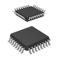
IC H8 MCU FLASH 8K 32-QFP
Manufacturer
Renesas Electronics America
Series
H8® H8/300H Tinyr
Datasheet
1.DF36912GFHV.pdf
(442 pages)
Specifications of HD64F36912GFH
Core Processor
H8/300H
Core Size
16-Bit
Speed
12MHz
Connectivity
I²C, SCI
Peripherals
LVD, POR, PWM, WDT
Number Of I /o
18
Program Memory Size
8KB (8K x 8)
Program Memory Type
FLASH
Ram Size
1.5K x 8
Voltage - Supply (vcc/vdd)
3 V ~ 5.5 V
Data Converters
A/D 4x10b
Oscillator Type
Internal
Operating Temperature
-20°C ~ 75°C
Package / Case
32-LQFP
Lead Free Status / RoHS Status
Contains lead / RoHS non-compliant
Eeprom Size
-
Available stocks
Company
Part Number
Manufacturer
Quantity
Price
Company:

Part Number:
HD64F36912GFH
Manufacturer:
Renesas Electronics America
Quantity:
10 000


Section 5 Clock Pulse Generators
Figure 5.1 Block Diagram of Clock Pulse Generators.................................................................. 69
Figure 5.2 State Transition of System Clock ................................................................................ 75
Figure 5.3 Flowchart of Clock Switching On-chip Oscillator Clock to External Clock (1) ........ 76
Figure 5.4 Flowchart of Clock Switching External Clock to On-chip Oscillator Clock (2) ......... 77
Figure 5.5 Timing Chart of Switching On-chip Oscillator Clock to External Clock.................... 78
Figure 5.6 Timing Chart to Switch External Clock to On-chip Oscillator Clock ......................... 79
Figure 5.7 Example of Trimming Flow for On-chip Oscillator Frequency .................................. 80
Figure 5.8 Timing Chart of Trimming of On-chip Oscillator Frequency ..................................... 81
Figure 5.9 Example of Connection to Crystal Resonator ............................................................. 82
Figure 5.10 Equivalent Circuit of Crystal Resonator.................................................................... 82
Figure 5.11 Example of Connection to Ceramic Resonator ......................................................... 83
Figure 5.12 Example of External Clock Input .............................................................................. 83
Figure 5.13 Example of Incorrect Board Design .......................................................................... 84
Section 6 Power-Down Modes
Figure 6.1 Mode Transition Diagram ........................................................................................... 91
Section 7 ROM
Figure 7.1 Flash Memory Block Configuration............................................................................ 98
Figure 7.2 Programming/Erasing Flowchart Example in User Program Mode.......................... 106
Figure 7.3 Program/Program-Verify Flowchart ......................................................................... 108
Figure 7.4 Erase/Erase-Verify Flowchart ................................................................................... 111
Section 9 I/O Ports
Figure 9.1 Port 1 Pin Configuration............................................................................................ 117
Figure 9.2 Port 2 Pin Configuration............................................................................................ 121
Figure 9.3 Port 5 Pin Configuration............................................................................................ 124
Figure 9.4 Port 7 Pin Configuration............................................................................................ 128
Figure 9.5 Port 8 Pin Configuration............................................................................................ 130
Figure 9.6 Port B Pin Configuration........................................................................................... 134
Figure 9.7 Port C Pin Configuration........................................................................................... 136
Section 10 Timer B1
Figure 10.1 Block Diagram of Timer B1.................................................................................... 139
Section 11 Timer V
Figure 11.1 Block Diagram of Timer V ..................................................................................... 146
Figure 11.2 Increment Timing with Internal Clock .................................................................... 153
Figure 11.3 Increment Timing with External Clock................................................................... 153
Figure 11.4 OVF Set Timing ...................................................................................................... 153
Figure 11.5 CMFA and CMFB Set Timing................................................................................ 154
Rev. 3.00 Sep. 14, 2006 Page xx of xxviii
Related parts for HD64F36912GFH
Image
Part Number
Description
Manufacturer
Datasheet
Request
R


Part Number:
Description:
KIT STARTER FOR M16C/29
Manufacturer:
Renesas Electronics America
Datasheet:

Part Number:
Description:
KIT STARTER FOR R8C/2D
Manufacturer:
Renesas Electronics America
Datasheet:

Part Number:
Description:
R0K33062P STARTER KIT
Manufacturer:
Renesas Electronics America
Datasheet:

Part Number:
Description:
KIT STARTER FOR R8C/23 E8A
Manufacturer:
Renesas Electronics America
Datasheet:

Part Number:
Description:
KIT STARTER FOR R8C/25
Manufacturer:
Renesas Electronics America
Datasheet:

Part Number:
Description:
KIT STARTER H8S2456 SHARPE DSPLY
Manufacturer:
Renesas Electronics America
Datasheet:

Part Number:
Description:
KIT STARTER FOR R8C38C
Manufacturer:
Renesas Electronics America
Datasheet:

Part Number:
Description:
KIT STARTER FOR R8C35C
Manufacturer:
Renesas Electronics America
Datasheet:

Part Number:
Description:
KIT STARTER FOR R8CL3AC+LCD APPS
Manufacturer:
Renesas Electronics America
Datasheet:
Part Number:
Description:
KIT STARTER FOR RX610
Manufacturer:
Renesas Electronics America
Datasheet:

Part Number:
Description:
KIT STARTER FOR R32C/118
Manufacturer:
Renesas Electronics America
Datasheet:

Part Number:
Description:
KIT DEV RSK-R8C/26-29
Manufacturer:
Renesas Electronics America
Datasheet:

Part Number:
Description:
KIT STARTER FOR SH7124
Manufacturer:
Renesas Electronics America
Datasheet:

Part Number:
Description:
KIT STARTER FOR H8SX/1622
Manufacturer:
Renesas Electronics America
Datasheet: