MMC2107CFCAG33 Freescale Semiconductor, MMC2107CFCAG33 Datasheet - Page 214
MMC2107CFCAG33
Manufacturer Part Number
MMC2107CFCAG33
Description
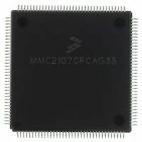
IC MCU 33MHZ 128K FLASH 144-LQFP
Manufacturer
Freescale Semiconductor
Series
MCorer
Datasheet
1.MMC2107CFCAF33.pdf
(618 pages)
Specifications of MMC2107CFCAG33
Core Processor
M210
Core Size
32-Bit
Speed
33MHz
Connectivity
EBI/EMI, SCI, SPI
Peripherals
POR, PWM, WDT
Number Of I /o
72
Program Memory Size
128KB (128K x 8)
Program Memory Type
FLASH
Ram Size
8K x 8
Voltage - Supply (vcc/vdd)
2.7 V ~ 3.6 V
Data Converters
A/D 8x10b
Oscillator Type
Internal
Operating Temperature
-40°C ~ 85°C
Package / Case
144-LQFP
Processor Series
MMC2107
Core
M-CORE
Data Bus Width
32 bit
Data Ram Size
8 KB
Interface Type
SCI/SPI
Maximum Clock Frequency
33 MHz
Number Of Programmable I/os
72
Number Of Timers
2
Operating Supply Voltage
0 V to 3.6 V
Maximum Operating Temperature
+ 85 C
Mounting Style
SMD/SMT
Minimum Operating Temperature
- 40 C
On-chip Adc
8-ch x 10-bit
Cpu Family
Mcore
Device Core
MCORE
Device Core Size
32b
Frequency (max)
33MHz
Total Internal Ram Size
8KB
# I/os (max)
72
Number Of Timers - General Purpose
2
Operating Supply Voltage (typ)
3.3/5V
Operating Supply Voltage (max)
3.6/5.5V
Operating Supply Voltage (min)
2.7/4.5V
Instruction Set Architecture
RISC
Operating Temp Range
-40C to 85C
Operating Temperature Classification
Industrial
Mounting
Surface Mount
Pin Count
144
Package Type
LQFP
Lead Free Status / RoHS Status
Lead free / RoHS Compliant
Eeprom Size
-
Lead Free Status / Rohs Status
Lead free / RoHS Compliant
Available stocks
Company
Part Number
Manufacturer
Quantity
Price
Company:

Part Number:
MMC2107CFCAG33
Manufacturer:
FREESCALE
Quantity:
210
Company:
Part Number:
MMC2107CFCAG33
Manufacturer:
freescaie
Quantity:
35
Company:
Part Number:
MMC2107CFCAG33
Manufacturer:
Freescale Semiconductor
Quantity:
10 000


Non-Volatile Memory FLASH (CMFR)
9.8.5 Erasing
Technical Data
214
NOTE:
To modify the charge stored in the isolated element of a bit from a logic 0
state to a logic 1 state, an erase operation is required. The erase
operation cannot change the logic 1 state to a logic 0 state; this transition
must be done by the program operation. Erase is a bulk operation that
affects the stored charge of all the isolated elements in an array block.
To make the block erasable, the array is divided into blocks that are
physically isolated from each other. Each of the array blocks may be
erased in isolation or in any combination. The array block size is fixed for
all blocks at 16 Kbytes and the module is comprised of eight blocks.
Array blocks that are protected (PROTECT[M] = 1) are not erased.
The array blocks selected for erase operation are determined by
BLOCK[7:0].
Erasing BLOCK 0 also erases the shadow information.
The erase sequence is outlined in
depicted in the flowchart form in
Freescale Semiconductor, Inc.
For More Information On This Product,
Non-Volatile Memory FLASH (CMFR)
Go to: www.freescale.com
Figure
9.8.5.1 Erase Sequence
9-9.
MMC2107 – Rev. 2.0
and
MOTOROLA
Related parts for MMC2107CFCAG33
Image
Part Number
Description
Manufacturer
Datasheet
Request
R

Part Number:
Description:
Manufacturer:
Freescale Semiconductor, Inc
Datasheet:
Part Number:
Description:
Manufacturer:
Freescale Semiconductor, Inc
Datasheet:
Part Number:
Description:
Manufacturer:
Freescale Semiconductor, Inc
Datasheet:
Part Number:
Description:
Manufacturer:
Freescale Semiconductor, Inc
Datasheet:
Part Number:
Description:
Manufacturer:
Freescale Semiconductor, Inc
Datasheet:
Part Number:
Description:
Manufacturer:
Freescale Semiconductor, Inc
Datasheet:
Part Number:
Description:
Manufacturer:
Freescale Semiconductor, Inc
Datasheet:
Part Number:
Description:
Manufacturer:
Freescale Semiconductor, Inc
Datasheet:
Part Number:
Description:
Manufacturer:
Freescale Semiconductor, Inc
Datasheet:
Part Number:
Description:
Manufacturer:
Freescale Semiconductor, Inc
Datasheet:
Part Number:
Description:
Manufacturer:
Freescale Semiconductor, Inc
Datasheet:
Part Number:
Description:
Manufacturer:
Freescale Semiconductor, Inc
Datasheet:
Part Number:
Description:
Manufacturer:
Freescale Semiconductor, Inc
Datasheet:
Part Number:
Description:
Manufacturer:
Freescale Semiconductor, Inc
Datasheet:
Part Number:
Description:
Manufacturer:
Freescale Semiconductor, Inc
Datasheet: