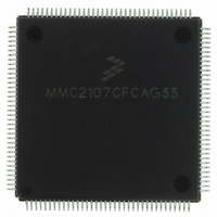
MMC2107CFCAG33 Freescale Semiconductor, MMC2107CFCAG33 Datasheet - Page 448

MMC2107CFCAG33
Manufacturer Part Number
MMC2107CFCAG33
Description
IC MCU 33MHZ 128K FLASH 144-LQFP
Manufacturer
Freescale Semiconductor
Series
MCorer
Datasheet
1.MMC2107CFCAF33.pdf
(618 pages)
Specifications of MMC2107CFCAG33
Core Processor
M210
Core Size
32-Bit
Speed
33MHz
Connectivity
EBI/EMI, SCI, SPI
Peripherals
POR, PWM, WDT
Number Of I /o
72
Program Memory Size
128KB (128K x 8)
Program Memory Type
FLASH
Ram Size
8K x 8
Voltage - Supply (vcc/vdd)
2.7 V ~ 3.6 V
Data Converters
A/D 8x10b
Oscillator Type
Internal
Operating Temperature
-40°C ~ 85°C
Package / Case
144-LQFP
Processor Series
MMC2107
Core
M-CORE
Data Bus Width
32 bit
Data Ram Size
8 KB
Interface Type
SCI/SPI
Maximum Clock Frequency
33 MHz
Number Of Programmable I/os
72
Number Of Timers
2
Operating Supply Voltage
0 V to 3.6 V
Maximum Operating Temperature
+ 85 C
Mounting Style
SMD/SMT
Minimum Operating Temperature
- 40 C
On-chip Adc
8-ch x 10-bit
Cpu Family
Mcore
Device Core
MCORE
Device Core Size
32b
Frequency (max)
33MHz
Total Internal Ram Size
8KB
# I/os (max)
72
Number Of Timers - General Purpose
2
Operating Supply Voltage (typ)
3.3/5V
Operating Supply Voltage (max)
3.6/5.5V
Operating Supply Voltage (min)
2.7/4.5V
Instruction Set Architecture
RISC
Operating Temp Range
-40C to 85C
Operating Temperature Classification
Industrial
Mounting
Surface Mount
Pin Count
144
Package Type
LQFP
Lead Free Status / RoHS Status
Lead free / RoHS Compliant
Eeprom Size
-
Lead Free Status / Rohs Status
Lead free / RoHS Compliant
Available stocks
Company
Part Number
Manufacturer
Quantity
Price
Company:
Part Number:
MMC2107CFCAG33
Manufacturer:
FREESCALE
Quantity:
210
Company:
Part Number:
MMC2107CFCAG33
Manufacturer:
freescaie
Quantity:
35
Company:
Part Number:
MMC2107CFCAG33
Manufacturer:
Freescale Semiconductor
Quantity:
10 000
- Current page: 448 of 618
- Download datasheet (8Mb)
Queued Analog-to-Digital Converter (QADC)
18.9.3.3 Channel Decode and Multiplexer
18.9.3.4 Sample Buffer
Technical Data
448
NOTE:
If the amplifier bypass mode is enabled for a conversion by setting the
amplifier bypass (BYP) field in the CCW, the timing changes to that
shown in
Table
eliminated, reducing the potential conversion time by two QCLKs. When
using the bypass mode, the external circuit should be of low source
impedance (typically less than 10 k ). Also, the loading effects to the
external circuitry by the QADC need to be considered, since the benefits
of the sample amplifier are not present.
Because of internal RC time constants, it is not recommended to use a
sample time of two QCLKs in bypass mode for high-frequency operation.
The internal multiplexer selects one of the eight analog input pins for
conversion. The selected input is connected to the Sample Buffer
Amplifier or to the sample capacitor. The multiplexer also includes
positive and negative stress protection circuitry, which prevents
deselected channels from affecting the selected channel when current is
injected into the deselected channels.
The sample buffer is used to raise the effective input impedance of the
A/D converter, so that external components (higher bandwidth or higher
impedance) are less critical to accuracy. The input voltage is buffered
onto the sample capacitor to reduce crosstalk between channels.
QCLK
Freescale Semiconductor, Inc.
For More Information On This Product,
Queued Analog-to-Digital Converter (QADC)
for more information on the BYP field. The initial sample time is
SAMPLE TIME
Figure
N CYCLES
(2,4,8,16)
SAMPLE
Figure 18-21. Bypass Mode Conversion Timing
TIME:
Go to: www.freescale.com
18-21. See
SUCCESSIVE-APPROXIMATION RESOLUTION SEQUENCE
18.8.7 Conversion Command Word
RESOLUTION
10 CYCLES
TIME:
MMC2107 – Rev. 2.0
MOTOROLA
Related parts for MMC2107CFCAG33
Image
Part Number
Description
Manufacturer
Datasheet
Request
R
Part Number:
Description:
Manufacturer:
Freescale Semiconductor, Inc
Datasheet:
Part Number:
Description:
Manufacturer:
Freescale Semiconductor, Inc
Datasheet:
Part Number:
Description:
Manufacturer:
Freescale Semiconductor, Inc
Datasheet:
Part Number:
Description:
Manufacturer:
Freescale Semiconductor, Inc
Datasheet:
Part Number:
Description:
Manufacturer:
Freescale Semiconductor, Inc
Datasheet:
Part Number:
Description:
Manufacturer:
Freescale Semiconductor, Inc
Datasheet:
Part Number:
Description:
Manufacturer:
Freescale Semiconductor, Inc
Datasheet:
Part Number:
Description:
Manufacturer:
Freescale Semiconductor, Inc
Datasheet:
Part Number:
Description:
Manufacturer:
Freescale Semiconductor, Inc
Datasheet:
Part Number:
Description:
Manufacturer:
Freescale Semiconductor, Inc
Datasheet:
Part Number:
Description:
Manufacturer:
Freescale Semiconductor, Inc
Datasheet:
Part Number:
Description:
Manufacturer:
Freescale Semiconductor, Inc
Datasheet:
Part Number:
Description:
Manufacturer:
Freescale Semiconductor, Inc
Datasheet:
Part Number:
Description:
Manufacturer:
Freescale Semiconductor, Inc
Datasheet:
Part Number:
Description:
Manufacturer:
Freescale Semiconductor, Inc
Datasheet:


