MMC2107CFCAG33 Freescale Semiconductor, MMC2107CFCAG33 Datasheet - Page 319
MMC2107CFCAG33
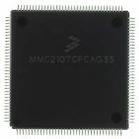
Manufacturer Part Number
MMC2107CFCAG33
Description
IC MCU 33MHZ 128K FLASH 144-LQFP
Manufacturer
Freescale Semiconductor
Series
MCorer
Datasheet
1.MMC2107CFCAF33.pdf
(618 pages)
Specifications of MMC2107CFCAG33
Core Processor
M210
Core Size
32-Bit
Speed
33MHz
Connectivity
EBI/EMI, SCI, SPI
Peripherals
POR, PWM, WDT
Number Of I /o
72
Program Memory Size
128KB (128K x 8)
Program Memory Type
FLASH
Ram Size
8K x 8
Voltage - Supply (vcc/vdd)
2.7 V ~ 3.6 V
Data Converters
A/D 8x10b
Oscillator Type
Internal
Operating Temperature
-40°C ~ 85°C
Package / Case
144-LQFP
Processor Series
MMC2107
Core
M-CORE
Data Bus Width
32 bit
Data Ram Size
8 KB
Interface Type
SCI/SPI
Maximum Clock Frequency
33 MHz
Number Of Programmable I/os
72
Number Of Timers
2
Operating Supply Voltage
0 V to 3.6 V
Maximum Operating Temperature
+ 85 C
Mounting Style
SMD/SMT
Minimum Operating Temperature
- 40 C
On-chip Adc
8-ch x 10-bit
Cpu Family
Mcore
Device Core
MCORE
Device Core Size
32b
Frequency (max)
33MHz
Total Internal Ram Size
8KB
# I/os (max)
72
Number Of Timers - General Purpose
2
Operating Supply Voltage (typ)
3.3/5V
Operating Supply Voltage (max)
3.6/5.5V
Operating Supply Voltage (min)
2.7/4.5V
Instruction Set Architecture
RISC
Operating Temp Range
-40C to 85C
Operating Temperature Classification
Industrial
Mounting
Surface Mount
Pin Count
144
Package Type
LQFP
Lead Free Status / RoHS Status
Lead free / RoHS Compliant
Eeprom Size
-
Lead Free Status / Rohs Status
Lead free / RoHS Compliant
Available stocks
Company
Part Number
Manufacturer
Quantity
Price
Company:

Part Number:
MMC2107CFCAG33
Manufacturer:
FREESCALE
Quantity:
210
Company:
Part Number:
MMC2107CFCAG33
Manufacturer:
freescaie
Quantity:
35
Company:
Part Number:
MMC2107CFCAG33
Manufacturer:
Freescale Semiconductor
Quantity:
10 000


15.7.18 Timer Port Data Register
MMC2107 – Rev. 2.0
MOTOROLA
Address: TIM1 — 0x00ce_001d
Reset:
Read: Anytime; read pin state when corresponding TIMDDR bit is 0;
read pin driver state when corresponding TIMDDR bit is 1
Write: Anytime
PORTT[3:0] — Timer Port Input Capture/Output Compare Data Bits
Read:
Write:
Data written to TIMPORT is buffered and drives the pins only when
they are configured as general-purpose outputs.
Reading an input (DDR bit = 0) reads the pin state; reading an output
(DDR bit = 1) reads the latch.
Writing to a pin configured as a timer output does not change the pin
state.
Freescale Semiconductor, Inc.
For More Information On This Product,
TIM2 — 0x00cf_001d
Figure 15-23. Timer Port Data Register (TIMPORT)
Bit 7
0
0
Timer Modules (TIM1 and TIM2)
Go to: www.freescale.com
= Writes have no effect and the access terminates without a transfer error exception.
6
0
0
5
0
0
4
0
0
PORTT3
3
0
Timer Modules (TIM1 and TIM2)
PORTT2
Memory Map and Registers
2
0
PORTT1
1
0
Technical Data
PORTT0
Bit 0
0
319
Related parts for MMC2107CFCAG33
Image
Part Number
Description
Manufacturer
Datasheet
Request
R

Part Number:
Description:
Manufacturer:
Freescale Semiconductor, Inc
Datasheet:
Part Number:
Description:
Manufacturer:
Freescale Semiconductor, Inc
Datasheet:
Part Number:
Description:
Manufacturer:
Freescale Semiconductor, Inc
Datasheet:
Part Number:
Description:
Manufacturer:
Freescale Semiconductor, Inc
Datasheet:
Part Number:
Description:
Manufacturer:
Freescale Semiconductor, Inc
Datasheet:
Part Number:
Description:
Manufacturer:
Freescale Semiconductor, Inc
Datasheet:
Part Number:
Description:
Manufacturer:
Freescale Semiconductor, Inc
Datasheet:
Part Number:
Description:
Manufacturer:
Freescale Semiconductor, Inc
Datasheet:
Part Number:
Description:
Manufacturer:
Freescale Semiconductor, Inc
Datasheet:
Part Number:
Description:
Manufacturer:
Freescale Semiconductor, Inc
Datasheet:
Part Number:
Description:
Manufacturer:
Freescale Semiconductor, Inc
Datasheet:
Part Number:
Description:
Manufacturer:
Freescale Semiconductor, Inc
Datasheet:
Part Number:
Description:
Manufacturer:
Freescale Semiconductor, Inc
Datasheet:
Part Number:
Description:
Manufacturer:
Freescale Semiconductor, Inc
Datasheet:
Part Number:
Description:
Manufacturer:
Freescale Semiconductor, Inc
Datasheet: