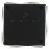
MMC2107CFCAG33 Freescale Semiconductor, MMC2107CFCAG33 Datasheet - Page 581

MMC2107CFCAG33
Manufacturer Part Number
MMC2107CFCAG33
Description
IC MCU 33MHZ 128K FLASH 144-LQFP
Manufacturer
Freescale Semiconductor
Series
MCorer
Datasheet
1.MMC2107CFCAF33.pdf
(618 pages)
Specifications of MMC2107CFCAG33
Core Processor
M210
Core Size
32-Bit
Speed
33MHz
Connectivity
EBI/EMI, SCI, SPI
Peripherals
POR, PWM, WDT
Number Of I /o
72
Program Memory Size
128KB (128K x 8)
Program Memory Type
FLASH
Ram Size
8K x 8
Voltage - Supply (vcc/vdd)
2.7 V ~ 3.6 V
Data Converters
A/D 8x10b
Oscillator Type
Internal
Operating Temperature
-40°C ~ 85°C
Package / Case
144-LQFP
Processor Series
MMC2107
Core
M-CORE
Data Bus Width
32 bit
Data Ram Size
8 KB
Interface Type
SCI/SPI
Maximum Clock Frequency
33 MHz
Number Of Programmable I/os
72
Number Of Timers
2
Operating Supply Voltage
0 V to 3.6 V
Maximum Operating Temperature
+ 85 C
Mounting Style
SMD/SMT
Minimum Operating Temperature
- 40 C
On-chip Adc
8-ch x 10-bit
Cpu Family
Mcore
Device Core
MCORE
Device Core Size
32b
Frequency (max)
33MHz
Total Internal Ram Size
8KB
# I/os (max)
72
Number Of Timers - General Purpose
2
Operating Supply Voltage (typ)
3.3/5V
Operating Supply Voltage (max)
3.6/5.5V
Operating Supply Voltage (min)
2.7/4.5V
Instruction Set Architecture
RISC
Operating Temp Range
-40C to 85C
Operating Temperature Classification
Industrial
Mounting
Surface Mount
Pin Count
144
Package Type
LQFP
Lead Free Status / RoHS Status
Lead free / RoHS Compliant
Eeprom Size
-
Lead Free Status / Rohs Status
Lead free / RoHS Compliant
Available stocks
Company
Part Number
Manufacturer
Quantity
Price
Company:
Part Number:
MMC2107CFCAG33
Manufacturer:
FREESCALE
Quantity:
210
Company:
Part Number:
MMC2107CFCAG33
Manufacturer:
freescaie
Quantity:
35
Company:
Part Number:
MMC2107CFCAG33
Manufacturer:
Freescale Semiconductor
Quantity:
10 000
- Current page: 581 of 618
- Download datasheet (8Mb)
21.14.14 Reserved Test Control Registers
21.14.15 Serial Protocol
MMC2107 – Rev. 2.0
MOTOROLA
CAUTION:
The FIFO is not affected by operations performed in debug mode,
except for incrementing the FIFO pointer when the FIFO is read. When
debug mode is entered, the FIFO counter points to the FIFO register
containing the address of the oldest of the eight change-of-flow
pre-fetches. The first FIFO read obtains the oldest address, and the
following FIFO reads return the other addresses from the oldest to the
newest, in order of execution.
To ensure FIFO coherence, a complete set of eight reads of the FIFO
must be performed. Each read increments the FIFO pointer, causing it
to point to the next location. After eight reads, the pointer points to the
same location as before the start of the read procedure.
The reserved test control registers (MEM_BIST, FTCR, and LSRL) are
reserved for factory testing.
To prevent damage to the device or system, do not access these
registers during normal operation.
The serial protocol permits an efficient means of communication
between the OnCE external command controller and the MCU. Before
starting any debugging activity, the external command controller must
wait for an acknowledgment that the device has entered debug mode.
The external command controller communicates with the device by
sending 8-bit commands to the OnCE command register and 16 to 128
bits of data to one of the other OnCE registers. Both commands and data
are sent or received LSB first. After sending a command, the external
command controller must wait for the processor to acknowledge
execution of certain commands before it can properly access another
OnCE register.
Freescale Semiconductor, Inc.
For More Information On This Product,
JTAG Test Access Port and OnCE
Go to: www.freescale.com
JTAG Test Access Port and OnCE
Functional Description
Technical Data
581
Related parts for MMC2107CFCAG33
Image
Part Number
Description
Manufacturer
Datasheet
Request
R
Part Number:
Description:
Manufacturer:
Freescale Semiconductor, Inc
Datasheet:
Part Number:
Description:
Manufacturer:
Freescale Semiconductor, Inc
Datasheet:
Part Number:
Description:
Manufacturer:
Freescale Semiconductor, Inc
Datasheet:
Part Number:
Description:
Manufacturer:
Freescale Semiconductor, Inc
Datasheet:
Part Number:
Description:
Manufacturer:
Freescale Semiconductor, Inc
Datasheet:
Part Number:
Description:
Manufacturer:
Freescale Semiconductor, Inc
Datasheet:
Part Number:
Description:
Manufacturer:
Freescale Semiconductor, Inc
Datasheet:
Part Number:
Description:
Manufacturer:
Freescale Semiconductor, Inc
Datasheet:
Part Number:
Description:
Manufacturer:
Freescale Semiconductor, Inc
Datasheet:
Part Number:
Description:
Manufacturer:
Freescale Semiconductor, Inc
Datasheet:
Part Number:
Description:
Manufacturer:
Freescale Semiconductor, Inc
Datasheet:
Part Number:
Description:
Manufacturer:
Freescale Semiconductor, Inc
Datasheet:
Part Number:
Description:
Manufacturer:
Freescale Semiconductor, Inc
Datasheet:
Part Number:
Description:
Manufacturer:
Freescale Semiconductor, Inc
Datasheet:
Part Number:
Description:
Manufacturer:
Freescale Semiconductor, Inc
Datasheet:


