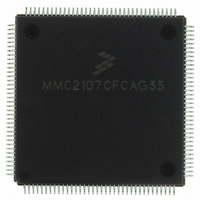
MMC2107CFCAG33 Freescale Semiconductor, MMC2107CFCAG33 Datasheet - Page 375

MMC2107CFCAG33
Manufacturer Part Number
MMC2107CFCAG33
Description
IC MCU 33MHZ 128K FLASH 144-LQFP
Manufacturer
Freescale Semiconductor
Series
MCorer
Datasheet
1.MMC2107CFCAF33.pdf
(618 pages)
Specifications of MMC2107CFCAG33
Core Processor
M210
Core Size
32-Bit
Speed
33MHz
Connectivity
EBI/EMI, SCI, SPI
Peripherals
POR, PWM, WDT
Number Of I /o
72
Program Memory Size
128KB (128K x 8)
Program Memory Type
FLASH
Ram Size
8K x 8
Voltage - Supply (vcc/vdd)
2.7 V ~ 3.6 V
Data Converters
A/D 8x10b
Oscillator Type
Internal
Operating Temperature
-40°C ~ 85°C
Package / Case
144-LQFP
Processor Series
MMC2107
Core
M-CORE
Data Bus Width
32 bit
Data Ram Size
8 KB
Interface Type
SCI/SPI
Maximum Clock Frequency
33 MHz
Number Of Programmable I/os
72
Number Of Timers
2
Operating Supply Voltage
0 V to 3.6 V
Maximum Operating Temperature
+ 85 C
Mounting Style
SMD/SMT
Minimum Operating Temperature
- 40 C
On-chip Adc
8-ch x 10-bit
Cpu Family
Mcore
Device Core
MCORE
Device Core Size
32b
Frequency (max)
33MHz
Total Internal Ram Size
8KB
# I/os (max)
72
Number Of Timers - General Purpose
2
Operating Supply Voltage (typ)
3.3/5V
Operating Supply Voltage (max)
3.6/5.5V
Operating Supply Voltage (min)
2.7/4.5V
Instruction Set Architecture
RISC
Operating Temp Range
-40C to 85C
Operating Temperature Classification
Industrial
Mounting
Surface Mount
Pin Count
144
Package Type
LQFP
Lead Free Status / RoHS Status
Lead free / RoHS Compliant
Eeprom Size
-
Lead Free Status / Rohs Status
Lead free / RoHS Compliant
Available stocks
Company
Part Number
Manufacturer
Quantity
Price
Company:
Part Number:
MMC2107CFCAG33
Manufacturer:
FREESCALE
Quantity:
210
Company:
Part Number:
MMC2107CFCAG33
Manufacturer:
freescaie
Quantity:
35
Company:
Part Number:
MMC2107CFCAG33
Manufacturer:
Freescale Semiconductor
Quantity:
10 000
- Current page: 375 of 618
- Download datasheet (8Mb)
17.6.3 SCK (Serial Clock)
17.6.4 SS (Slave Select)
17.7 Memory Map and Registers
MMC2107 – Rev. 2.0
MOTOROLA
NOTE:
The SCK pin is the serial clock pin for synchronizing transmissions
between master and slave devices. In master mode, SCK is an output.
In slave mode, SCK is an input.
In a multiple-master system, all SCK pins are tied together.
In master mode, the SS pin can be:
In slave mode, the SS pin is always a slave-select input.
Table 17-2
Reading reserved addresses (0x00cb_004 and 0x00cb_0009 through
0x00cb_000b) and unimplemented addresses (0x00cb_000c through
0x00cb_000f) returns 0s. Writing to unimplemented addresses has no
effect. Accessing unimplemented addresses does not generate an error
response.
1. S/U = CPU supervisor or user mode access. User mode accesses to supervisor only
•
•
•
•
Freescale Semiconductor, Inc.
0x00cb_0000
0x00cb_0001
0x00cb_0002
0x00cb_0003
0x00cb_0005
0x00cb_0006
0x00cb_0007
0x00cb_0008
addresses have no effect and result in a cycle termination transfer error.
For More Information On This Product,
Address
A mode-fault input
A general-purpose input
A general-purpose output
A slave-select output
Serial Peripheral Interface Module (SPI)
shows the SPI memory map.
Go to: www.freescale.com
SPI pullup and reduced drive register (SPIPURD)
Table 17-2. SPI Memory Map
SPI port data direction register (SPIDDR)
SPI port data register (SPIPORT)
SPI control register 1 (SPICR1)
SPI control register 2 (SPICR2)
SPI baud rate register (SPIBR)
SPI status register (SPISR)
SPI data register (SPIDR)
Bits 7–0
Serial Peripheral Interface Module (SPI)
Memory Map and Registers
Technical Data
Access
S/U
S/U
S/U
S/U
S/U
S/U
S/U
S/U
375
(1)
Related parts for MMC2107CFCAG33
Image
Part Number
Description
Manufacturer
Datasheet
Request
R
Part Number:
Description:
Manufacturer:
Freescale Semiconductor, Inc
Datasheet:
Part Number:
Description:
Manufacturer:
Freescale Semiconductor, Inc
Datasheet:
Part Number:
Description:
Manufacturer:
Freescale Semiconductor, Inc
Datasheet:
Part Number:
Description:
Manufacturer:
Freescale Semiconductor, Inc
Datasheet:
Part Number:
Description:
Manufacturer:
Freescale Semiconductor, Inc
Datasheet:
Part Number:
Description:
Manufacturer:
Freescale Semiconductor, Inc
Datasheet:
Part Number:
Description:
Manufacturer:
Freescale Semiconductor, Inc
Datasheet:
Part Number:
Description:
Manufacturer:
Freescale Semiconductor, Inc
Datasheet:
Part Number:
Description:
Manufacturer:
Freescale Semiconductor, Inc
Datasheet:
Part Number:
Description:
Manufacturer:
Freescale Semiconductor, Inc
Datasheet:
Part Number:
Description:
Manufacturer:
Freescale Semiconductor, Inc
Datasheet:
Part Number:
Description:
Manufacturer:
Freescale Semiconductor, Inc
Datasheet:
Part Number:
Description:
Manufacturer:
Freescale Semiconductor, Inc
Datasheet:
Part Number:
Description:
Manufacturer:
Freescale Semiconductor, Inc
Datasheet:
Part Number:
Description:
Manufacturer:
Freescale Semiconductor, Inc
Datasheet:


