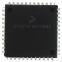
MMC2107CFCAG33 Freescale Semiconductor, MMC2107CFCAG33 Datasheet - Page 414

MMC2107CFCAG33
Manufacturer Part Number
MMC2107CFCAG33
Description
IC MCU 33MHZ 128K FLASH 144-LQFP
Manufacturer
Freescale Semiconductor
Series
MCorer
Datasheet
1.MMC2107CFCAF33.pdf
(618 pages)
Specifications of MMC2107CFCAG33
Core Processor
M210
Core Size
32-Bit
Speed
33MHz
Connectivity
EBI/EMI, SCI, SPI
Peripherals
POR, PWM, WDT
Number Of I /o
72
Program Memory Size
128KB (128K x 8)
Program Memory Type
FLASH
Ram Size
8K x 8
Voltage - Supply (vcc/vdd)
2.7 V ~ 3.6 V
Data Converters
A/D 8x10b
Oscillator Type
Internal
Operating Temperature
-40°C ~ 85°C
Package / Case
144-LQFP
Processor Series
MMC2107
Core
M-CORE
Data Bus Width
32 bit
Data Ram Size
8 KB
Interface Type
SCI/SPI
Maximum Clock Frequency
33 MHz
Number Of Programmable I/os
72
Number Of Timers
2
Operating Supply Voltage
0 V to 3.6 V
Maximum Operating Temperature
+ 85 C
Mounting Style
SMD/SMT
Minimum Operating Temperature
- 40 C
On-chip Adc
8-ch x 10-bit
Cpu Family
Mcore
Device Core
MCORE
Device Core Size
32b
Frequency (max)
33MHz
Total Internal Ram Size
8KB
# I/os (max)
72
Number Of Timers - General Purpose
2
Operating Supply Voltage (typ)
3.3/5V
Operating Supply Voltage (max)
3.6/5.5V
Operating Supply Voltage (min)
2.7/4.5V
Instruction Set Architecture
RISC
Operating Temp Range
-40C to 85C
Operating Temperature Classification
Industrial
Mounting
Surface Mount
Pin Count
144
Package Type
LQFP
Lead Free Status / RoHS Status
Lead free / RoHS Compliant
Eeprom Size
-
Lead Free Status / Rohs Status
Lead free / RoHS Compliant
Available stocks
Company
Part Number
Manufacturer
Quantity
Price
Company:
Part Number:
MMC2107CFCAG33
Manufacturer:
FREESCALE
Quantity:
210
Company:
Part Number:
MMC2107CFCAG33
Manufacturer:
freescaie
Quantity:
35
Company:
Part Number:
MMC2107CFCAG33
Manufacturer:
Freescale Semiconductor
Quantity:
10 000
- Current page: 414 of 618
- Download datasheet (8Mb)
Queued Analog-to-Digital Converter (QADC)
18.8.4 Port QA Data Direction Register
Technical Data
414
NOTE:
The port data direction register (DDRQA) is associated with the port QA
digital I/O pins. The bidirectional pins may have somewhat higher
leakage and capacitance specifications. Any bit in this register set to 1
configures the corresponding pin as an output. Any bit in this register
cleared to 0 configures the corresponding pin as an input. The software
is responsible for ensuring that DDR bits are not set to 1 on pins used for
analog inputs. When the DDR bit is set to 1 and the pin is selected for
analog conversion, the voltage sampled is that of the output digital driver
as influenced by the load.
When the MUX (externally multiplexed) bit is set in QACR0, the data
direction register settings are ignored for the bits corresponding to
PQA[1:0], the two multiplexed address (MA[1:0]) output pins. The
MA[1:0] pins are forced to be digital outputs, regardless of the data
direction setting, and the multiplexed address outputs are driven. The
data returned during a port data register read is the value of MA[1:0],
regardless of the data direction setting.
Similarly, when the external trigger pins are assigned to port pins and
external trigger queue operating mode is selected, the data direction
setting for the corresponding pins, PQA3 or PQA4, is ignored. The port
pins are forced to be digital inputs for ETRIG1 and/or ETRIG2. The data
driven during a port data register read is the actual value of the pin,
regardless of the data direction setting.
Use caution when mixing digital and analog inputs. They should be
isolated as much as possible. Rise and fall times should be as large as
possible to minimize ac coupling effects.
Since port QB is input-only, a data direction register is not needed.
Therefore, the lower byte of the port data direction register is not
implemented.
Freescale Semiconductor, Inc.
For More Information On This Product,
Queued Analog-to-Digital Converter (QADC)
Go to: www.freescale.com
MMC2107 – Rev. 2.0
MOTOROLA
Related parts for MMC2107CFCAG33
Image
Part Number
Description
Manufacturer
Datasheet
Request
R
Part Number:
Description:
Manufacturer:
Freescale Semiconductor, Inc
Datasheet:
Part Number:
Description:
Manufacturer:
Freescale Semiconductor, Inc
Datasheet:
Part Number:
Description:
Manufacturer:
Freescale Semiconductor, Inc
Datasheet:
Part Number:
Description:
Manufacturer:
Freescale Semiconductor, Inc
Datasheet:
Part Number:
Description:
Manufacturer:
Freescale Semiconductor, Inc
Datasheet:
Part Number:
Description:
Manufacturer:
Freescale Semiconductor, Inc
Datasheet:
Part Number:
Description:
Manufacturer:
Freescale Semiconductor, Inc
Datasheet:
Part Number:
Description:
Manufacturer:
Freescale Semiconductor, Inc
Datasheet:
Part Number:
Description:
Manufacturer:
Freescale Semiconductor, Inc
Datasheet:
Part Number:
Description:
Manufacturer:
Freescale Semiconductor, Inc
Datasheet:
Part Number:
Description:
Manufacturer:
Freescale Semiconductor, Inc
Datasheet:
Part Number:
Description:
Manufacturer:
Freescale Semiconductor, Inc
Datasheet:
Part Number:
Description:
Manufacturer:
Freescale Semiconductor, Inc
Datasheet:
Part Number:
Description:
Manufacturer:
Freescale Semiconductor, Inc
Datasheet:
Part Number:
Description:
Manufacturer:
Freescale Semiconductor, Inc
Datasheet:


