MMC2107CFCAG33 Freescale Semiconductor, MMC2107CFCAG33 Datasheet - Page 539
MMC2107CFCAG33
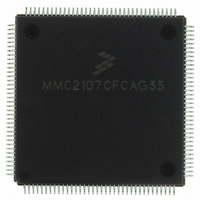
Manufacturer Part Number
MMC2107CFCAG33
Description
IC MCU 33MHZ 128K FLASH 144-LQFP
Manufacturer
Freescale Semiconductor
Series
MCorer
Datasheet
1.MMC2107CFCAF33.pdf
(618 pages)
Specifications of MMC2107CFCAG33
Core Processor
M210
Core Size
32-Bit
Speed
33MHz
Connectivity
EBI/EMI, SCI, SPI
Peripherals
POR, PWM, WDT
Number Of I /o
72
Program Memory Size
128KB (128K x 8)
Program Memory Type
FLASH
Ram Size
8K x 8
Voltage - Supply (vcc/vdd)
2.7 V ~ 3.6 V
Data Converters
A/D 8x10b
Oscillator Type
Internal
Operating Temperature
-40°C ~ 85°C
Package / Case
144-LQFP
Processor Series
MMC2107
Core
M-CORE
Data Bus Width
32 bit
Data Ram Size
8 KB
Interface Type
SCI/SPI
Maximum Clock Frequency
33 MHz
Number Of Programmable I/os
72
Number Of Timers
2
Operating Supply Voltage
0 V to 3.6 V
Maximum Operating Temperature
+ 85 C
Mounting Style
SMD/SMT
Minimum Operating Temperature
- 40 C
On-chip Adc
8-ch x 10-bit
Cpu Family
Mcore
Device Core
MCORE
Device Core Size
32b
Frequency (max)
33MHz
Total Internal Ram Size
8KB
# I/os (max)
72
Number Of Timers - General Purpose
2
Operating Supply Voltage (typ)
3.3/5V
Operating Supply Voltage (max)
3.6/5.5V
Operating Supply Voltage (min)
2.7/4.5V
Instruction Set Architecture
RISC
Operating Temp Range
-40C to 85C
Operating Temperature Classification
Industrial
Mounting
Surface Mount
Pin Count
144
Package Type
LQFP
Lead Free Status / RoHS Status
Lead free / RoHS Compliant
Eeprom Size
-
Lead Free Status / Rohs Status
Lead free / RoHS Compliant
Available stocks
Company
Part Number
Manufacturer
Quantity
Price
Company:

Part Number:
MMC2107CFCAG33
Manufacturer:
FREESCALE
Quantity:
210
Company:
Part Number:
MMC2107CFCAG33
Manufacturer:
freescaie
Quantity:
35
Company:
Part Number:
MMC2107CFCAG33
Manufacturer:
Freescale Semiconductor
Quantity:
10 000


MMC2107 – Rev. 2.0
MOTOROLA
NOTE:
As an input, this signal provides multiple functions such as:
If used to enter debug mode, DE must be pulled negated before the
processor exits debug mode to prevent a still low signal from being
unintentionally recognized as another debug request. Also, asserting
this signal to enter debug mode may prevent external logic from seeing
the processor output acknowledgment since the external pullup may not
be able to pull the signal negated before the handshake is asserted.
Finally, if using this signal to enable OnCE outside of reset it may be
seen as a request to enter debug mode.
•
•
•
Freescale Semiconductor, Inc.
For More Information On This Product,
The main function is a means of entering debug mode from an
external command controller. This signal, when asserted, causes
the CPU to finish the current instruction being executed, save the
instruction pipeline information, enter debug mode, and wait for
commands to be entered from the serial debug input line. This
input must be asserted for at least three system clocks, sampled
with the rising CLKOUT edge. This function is ignored during
reset. While the processor is in debug mode, this signal is still
sampled but has no effect until debug mode is exited.
Another input function is to enable OnCE. This is an alternate
method to the ENABLE_MCU_ONCE JTAG command to enable
the OnCE logic to be accessible via the JTAG interface. This input
signal must be asserted low (while in the test-logic-reset state with
POR/TRST not asserted) for at least two TCLK rising edges. Once
enabled, the OnCE will remain enabled until the next POR or
TRST resets.
Another input function is as a wake-up event from a low-power
mode of operation. Asynchronously asserting this signal will cause
the clock controller to restart. This signal must be held asserted
until the M•CORE receives three valid rising edges on the system
clock. Then the processor will exit the low-power mode and go into
debug mode.
JTAG Test Access Port and OnCE
Go to: www.freescale.com
JTAG Test Access Port and OnCE
Top-Level Test Access Port (TAP)
Technical Data
539
Related parts for MMC2107CFCAG33
Image
Part Number
Description
Manufacturer
Datasheet
Request
R

Part Number:
Description:
Manufacturer:
Freescale Semiconductor, Inc
Datasheet:
Part Number:
Description:
Manufacturer:
Freescale Semiconductor, Inc
Datasheet:
Part Number:
Description:
Manufacturer:
Freescale Semiconductor, Inc
Datasheet:
Part Number:
Description:
Manufacturer:
Freescale Semiconductor, Inc
Datasheet:
Part Number:
Description:
Manufacturer:
Freescale Semiconductor, Inc
Datasheet:
Part Number:
Description:
Manufacturer:
Freescale Semiconductor, Inc
Datasheet:
Part Number:
Description:
Manufacturer:
Freescale Semiconductor, Inc
Datasheet:
Part Number:
Description:
Manufacturer:
Freescale Semiconductor, Inc
Datasheet:
Part Number:
Description:
Manufacturer:
Freescale Semiconductor, Inc
Datasheet:
Part Number:
Description:
Manufacturer:
Freescale Semiconductor, Inc
Datasheet:
Part Number:
Description:
Manufacturer:
Freescale Semiconductor, Inc
Datasheet:
Part Number:
Description:
Manufacturer:
Freescale Semiconductor, Inc
Datasheet:
Part Number:
Description:
Manufacturer:
Freescale Semiconductor, Inc
Datasheet:
Part Number:
Description:
Manufacturer:
Freescale Semiconductor, Inc
Datasheet:
Part Number:
Description:
Manufacturer:
Freescale Semiconductor, Inc
Datasheet: