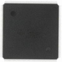
HD6417727F160CV Renesas Electronics America, HD6417727F160CV Datasheet - Page 106

HD6417727F160CV
Manufacturer Part Number
HD6417727F160CV
Description
IC SH MPU ROMLESS 240QFN
Manufacturer
Renesas Electronics America
Series
SuperH® SH7700r
Datasheet
1.HD6417727BP100CV.pdf
(1098 pages)
Specifications of HD6417727F160CV
Core Processor
SH-3 DSP
Core Size
32-Bit
Speed
160MHz
Connectivity
FIFO, SCI, SIO, SmartCard, USB
Peripherals
DMA, LCD, POR, WDT
Number Of I /o
104
Program Memory Type
ROMless
Ram Size
32K x 8
Voltage - Supply (vcc/vdd)
1.7 V ~ 2.05 V
Data Converters
A/D 6x10b; D/A 2x8b
Oscillator Type
Internal
Operating Temperature
-20°C ~ 75°C
Package / Case
240-QFP
Lead Free Status / RoHS Status
Lead free / RoHS Compliant
Eeprom Size
-
Program Memory Size
-
Available stocks
Company
Part Number
Manufacturer
Quantity
Price
Company:
Part Number:
HD6417727F160CV
Manufacturer:
RENESAS
Quantity:
37
Company:
Part Number:
HD6417727F160CV
Manufacturer:
RENESAS
Quantity:
753
- Current page: 106 of 1098
- Download datasheet (7Mb)
Section 2 CPU
2.4.2
Two different memory accesses are made with DSP instructions. The two kinds of instructions are
X and Y data transfer instructions (MOVX.W, MOVY.W) and single data transfer instructions
(MOVS.W, MOVSL). The data addressing is different for these two kinds of instruction. An
overview of the data transfer instructions is given in table 2.13.
Table 2.13 Overview of Data Transfer Instructions
Address register
Index register
Addressing
Modulo addressing
Data bus
Data length
Bus contention
Memory
Source register
Destination register
X/Y Data Addressing: With DSP instructions, the X and Y data memory can be accessed
simultaneously using the MOVX.W and MOVY.W instructions. Two address pointers are
provided for DSP instructions to enable simultaneous access to X and Y data memory. Only
pointer addressing can be used with DSP instructions; immediate addressing is not available.
Address registers are divided into two, with register R4 or R5 functioning as the X memory
address register (Ax), and register R6 or R7 as the Y memory address register (Ay). The following
three kinds of addressing can be used with X and Y data transfer instructions.
1. Non-update address register addressing:
Rev.6.00 Mar. 27, 2009 Page 48 of 1036
REJ09B0254-0600
The Ax and Ay registers are address pointers. They are not updated.
DSP Data Addressing
X/Y Data Transfer Processing
(MOVX.W, MOVY.W)
Ax: R4, R5, Ay: R6, R7
Ix: R8, Iy: R9
Nop/Inc (+2)/index addition:
post-increment
—
Possible
XDB, YDB
16 bits (word)
No
X/Y data memory
Dx, Dy: A0, A1
Dx: X0/X1, Dy: Y0/Y1
Single Data Transfer Processing
(MOVS.W, MOVS.L)
Nop/Inc (+2, +4)/index addition:
post-increment
Dec (–2, –4): pre-decrement
Not possible
A0G, A1G
A0G, A1G
As: R2, R3, R4, R5
Is: R8
LDB
16/32 bits (word/longword)
Yes
Entire memory space
Ds: A0/A1, M0/M1, X0/X1, Y0/Y1,
Ds: A0/A1, M0/M1, X0/X1, Y0/Y1,
Related parts for HD6417727F160CV
Image
Part Number
Description
Manufacturer
Datasheet
Request
R

Part Number:
Description:
KIT STARTER FOR M16C/29
Manufacturer:
Renesas Electronics America
Datasheet:

Part Number:
Description:
KIT STARTER FOR R8C/2D
Manufacturer:
Renesas Electronics America
Datasheet:

Part Number:
Description:
R0K33062P STARTER KIT
Manufacturer:
Renesas Electronics America
Datasheet:

Part Number:
Description:
KIT STARTER FOR R8C/23 E8A
Manufacturer:
Renesas Electronics America
Datasheet:

Part Number:
Description:
KIT STARTER FOR R8C/25
Manufacturer:
Renesas Electronics America
Datasheet:

Part Number:
Description:
KIT STARTER H8S2456 SHARPE DSPLY
Manufacturer:
Renesas Electronics America
Datasheet:

Part Number:
Description:
KIT STARTER FOR R8C38C
Manufacturer:
Renesas Electronics America
Datasheet:

Part Number:
Description:
KIT STARTER FOR R8C35C
Manufacturer:
Renesas Electronics America
Datasheet:

Part Number:
Description:
KIT STARTER FOR R8CL3AC+LCD APPS
Manufacturer:
Renesas Electronics America
Datasheet:

Part Number:
Description:
KIT STARTER FOR RX610
Manufacturer:
Renesas Electronics America
Datasheet:

Part Number:
Description:
KIT STARTER FOR R32C/118
Manufacturer:
Renesas Electronics America
Datasheet:

Part Number:
Description:
KIT DEV RSK-R8C/26-29
Manufacturer:
Renesas Electronics America
Datasheet:

Part Number:
Description:
KIT STARTER FOR SH7124
Manufacturer:
Renesas Electronics America
Datasheet:

Part Number:
Description:
KIT STARTER FOR H8SX/1622
Manufacturer:
Renesas Electronics America
Datasheet:

Part Number:
Description:
KIT DEV FOR SH7203
Manufacturer:
Renesas Electronics America
Datasheet:


