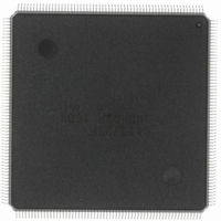
HD6417727F160CV Renesas Electronics America, HD6417727F160CV Datasheet - Page 364

HD6417727F160CV
Manufacturer Part Number
HD6417727F160CV
Description
IC SH MPU ROMLESS 240QFN
Manufacturer
Renesas Electronics America
Series
SuperH® SH7700r
Datasheet
1.HD6417727BP100CV.pdf
(1098 pages)
Specifications of HD6417727F160CV
Core Processor
SH-3 DSP
Core Size
32-Bit
Speed
160MHz
Connectivity
FIFO, SCI, SIO, SmartCard, USB
Peripherals
DMA, LCD, POR, WDT
Number Of I /o
104
Program Memory Type
ROMless
Ram Size
32K x 8
Voltage - Supply (vcc/vdd)
1.7 V ~ 2.05 V
Data Converters
A/D 6x10b; D/A 2x8b
Oscillator Type
Internal
Operating Temperature
-20°C ~ 75°C
Package / Case
240-QFP
Lead Free Status / RoHS Status
Lead free / RoHS Compliant
Eeprom Size
-
Program Memory Size
-
Available stocks
Company
Part Number
Manufacturer
Quantity
Price
Company:
Part Number:
HD6417727F160CV
Manufacturer:
RENESAS
Quantity:
37
Company:
Part Number:
HD6417727F160CV
Manufacturer:
RENESAS
Quantity:
753
- Current page: 364 of 1098
- Download datasheet (7Mb)
Section 12 Bus State Controller (BSC)
Bit 2—Refresh Control (RFSH): The RFSH bit determines whether or not the refresh operation
of the synchronous DRAM is performed. The timer for generation of the refresh request frequency
can also be used as an interval timer.
Bit 2: RFSH
0
1
Bit 1—Refresh Mode (RMODE): The RMODE bit selects whether to perform an ordinary
refresh or a self-refresh when the RFSH bit is 1. When the RFSH bit is 1 and this bit is 0, a CAS-
before-RAS refresh or an auto-refresh is performed on synchronous DRAM at the period set by
the refresh-related registers RTCNT, RTCOR and RTCSR. When a refresh request occurs during
an external bus cycle, the bus cycle will be ended and the refresh cycle performed. When the
RFSH bit is 1 and this bit is also 1, the synchronous DRAM will wait for the end of any executing
external bus cycle before going into a self-refresh. All refresh requests to memory that is in the
self-refresh state are ignored.
Bit 1: RMODE
0
1
Bit 0—Reserved: This bit is always read as 0. The write value should always be 0.
12.2.6
The PCMCIA control register (RCR) specifies the assert/negate timing of the OE and WE signals
(RD and WE1 pins of this LSI) for the PCMCIA interface connected to areas 5 and 6. Note that
the assertion widths of OE and WE are set using the wait control bits of the WCR2 register.
The PCR register is a 16-bit read/write register. It is initialized at a power-on reset to H'0000.
However, the register is not initialized and the contents remain unchanged at a manual reset and
when in standby mode.
Rev.6.00 Mar. 27, 2009 Page 306 of 1036
REJ09B0254-0600
Initial value:
R/W: R/W
Bit:
PCMCIA Control Register (PCR)
W3
A6
15
0
R/W
W3
A5
14
0
Description
No refresh
Refresh
Description
CAS-before-RAS refresh (RFSH must be 1)
Self-refresh (RFSH must be 1)
R/W
13
—
0
R/W
12
—
0
TED2
R/W
11
A5
0
TED2
R/W
A6
10
0
TEH2
R/W
A5
9
0
TEH2
R/W
A6
0
8
TED1
R/W
A5
7
0
TED0
R/W
A5
0
6
TED1
R/W
A6
5
0
TED0
R/W
A6
0
4
TEH1
R/W
A5
3
0
TEH0
R/W
A5
2
0
(Initial value)
(Initial value)
TEH1
R/W
A6
1
0
TEH0
R/W
A6
0
0
Related parts for HD6417727F160CV
Image
Part Number
Description
Manufacturer
Datasheet
Request
R

Part Number:
Description:
KIT STARTER FOR M16C/29
Manufacturer:
Renesas Electronics America
Datasheet:

Part Number:
Description:
KIT STARTER FOR R8C/2D
Manufacturer:
Renesas Electronics America
Datasheet:

Part Number:
Description:
R0K33062P STARTER KIT
Manufacturer:
Renesas Electronics America
Datasheet:

Part Number:
Description:
KIT STARTER FOR R8C/23 E8A
Manufacturer:
Renesas Electronics America
Datasheet:

Part Number:
Description:
KIT STARTER FOR R8C/25
Manufacturer:
Renesas Electronics America
Datasheet:

Part Number:
Description:
KIT STARTER H8S2456 SHARPE DSPLY
Manufacturer:
Renesas Electronics America
Datasheet:

Part Number:
Description:
KIT STARTER FOR R8C38C
Manufacturer:
Renesas Electronics America
Datasheet:

Part Number:
Description:
KIT STARTER FOR R8C35C
Manufacturer:
Renesas Electronics America
Datasheet:

Part Number:
Description:
KIT STARTER FOR R8CL3AC+LCD APPS
Manufacturer:
Renesas Electronics America
Datasheet:

Part Number:
Description:
KIT STARTER FOR RX610
Manufacturer:
Renesas Electronics America
Datasheet:

Part Number:
Description:
KIT STARTER FOR R32C/118
Manufacturer:
Renesas Electronics America
Datasheet:

Part Number:
Description:
KIT DEV RSK-R8C/26-29
Manufacturer:
Renesas Electronics America
Datasheet:

Part Number:
Description:
KIT STARTER FOR SH7124
Manufacturer:
Renesas Electronics America
Datasheet:

Part Number:
Description:
KIT STARTER FOR H8SX/1622
Manufacturer:
Renesas Electronics America
Datasheet:

Part Number:
Description:
KIT DEV FOR SH7203
Manufacturer:
Renesas Electronics America
Datasheet:


