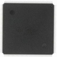
HD6417727F160CV Renesas Electronics America, HD6417727F160CV Datasheet - Page 381

HD6417727F160CV
Manufacturer Part Number
HD6417727F160CV
Description
IC SH MPU ROMLESS 240QFN
Manufacturer
Renesas Electronics America
Series
SuperH® SH7700r
Datasheet
1.HD6417727BP100CV.pdf
(1098 pages)
Specifications of HD6417727F160CV
Core Processor
SH-3 DSP
Core Size
32-Bit
Speed
160MHz
Connectivity
FIFO, SCI, SIO, SmartCard, USB
Peripherals
DMA, LCD, POR, WDT
Number Of I /o
104
Program Memory Type
ROMless
Ram Size
32K x 8
Voltage - Supply (vcc/vdd)
1.7 V ~ 2.05 V
Data Converters
A/D 6x10b; D/A 2x8b
Oscillator Type
Internal
Operating Temperature
-20°C ~ 75°C
Package / Case
240-QFP
Lead Free Status / RoHS Status
Lead free / RoHS Compliant
Eeprom Size
-
Program Memory Size
-
Available stocks
Company
Part Number
Manufacturer
Quantity
Price
Company:
Part Number:
HD6417727F160CV
Manufacturer:
RENESAS
Quantity:
37
Company:
Part Number:
HD6417727F160CV
Manufacturer:
RENESAS
Quantity:
753
- Current page: 381 of 1098
- Download datasheet (7Mb)
Section 12 Bus State Controller (BSC)
When synchronous DRAM is connected, the RAS signal, CAS signal, RD/WR signal, and byte
controls DQMHH, DQMHL, DQMLH, and DQMLL are all asserted and addresses multiplexed.
Control of RAS, CAS, data timing, and address multiplexing is set with MCR.
Area 3: Area 3 physical addresses A28 to A26 are 011. Addresses A31 to A29 are ignored and the
address range is H'0C000000 + H'20000000 × n to H'0FFFFFFF + H'20000000 × n (n = 0 to 6 and
n = 1 to 6 are the shadow spaces).
Ordinary memories like SRAM and ROM, as well as synchronous DRAM, can be connected to
this space. Byte, word or longword can be selected as the bus width using the A3SZ1 to A3SZ0
bits of BCR2 for ordinary memory. When area 3 space is accessed, CS3 is asserted.
When ordinary memories are connected, an RD signal that can be used as OE and the WE0 to
WE3 signals for write control are asserted and the number of bus cycles is selected between 0 and
3 wait cycles using the A3W1 to A3W0 bits of WCR2. In addition, any number of waits can be
inserted in each bus cycle by means of the external wait pin (WAIT).only when the ordinary
memories are connected.
When synchronous DRAM is connected, the RAS signal, CAS signal, RD/WR signal, and byte
controls DQMHH, DQMHL, DQMLH, and DQMLL are all asserted and addresses multiplexed.
Area 4: Area 4 physical addresses A28 to A26 are 1'0. AddressesA31 to A29 are ignored and the
address range is H'10000000 + H'20000000 × n – H'13FFFFFF + H'20000000 × n (n = 0 to 6 and
n = 1 to 6 are the shadow spaces).
Only ordinary memories like SRAM and ROM can be connected to this space. Byte, word, or
longword can be selected as the bus width using the A4SZ1 to A4SZ0 bits of BCR2. When the
area 4 space is accessed, a CS4 signal is asserted. An RD signal that can be used as OE and the
WE0 to WE3 signals for write control are also asserted. The number of bus cycles is selected
between 0 and 10 wait cycles using the A4W2 to A4W0 bits of WCR2. In addition, any number
of waits can be inserted in each bus cycle by means of the external wait pin (WAIT).
Area 5: Area 5 physical addresses A28 to A26 are 101. Addresses A31 to A29 are ignored and the
address range is the 64 Mbytes at H'14000000 + H'20000000 × n to H'17FFFFFF + H'20000000 ×
n (n = 0 to 6 and n = 1 to 6 are the shadow spaces).
Ordinary memories like SRAM and ROM as well as burst ROM and PCMCIA interfaces can be
connected to this space. When the PCMCIA interface is used, the IC memory card interface
address range-comprises the 32 Mbytes at H'14000000 + H'20000000 × n to H'15FFFFFF +
H'20000000 × n (n = 0 to 6 and n = 1 to 6 are the shadow spaces), and the I/O card interface
address range-comprises the 32 Mbytes at H'16000000 + H'20000000 × n to H'17FFFFFF +
H'20000000 × n (n = 0 to 6 and n = 1 to 6 are the shadow spaces).
Rev.6.00 Mar. 27, 2009 Page 323 of 1036
REJ09B0254-0600
Related parts for HD6417727F160CV
Image
Part Number
Description
Manufacturer
Datasheet
Request
R

Part Number:
Description:
KIT STARTER FOR M16C/29
Manufacturer:
Renesas Electronics America
Datasheet:

Part Number:
Description:
KIT STARTER FOR R8C/2D
Manufacturer:
Renesas Electronics America
Datasheet:

Part Number:
Description:
R0K33062P STARTER KIT
Manufacturer:
Renesas Electronics America
Datasheet:

Part Number:
Description:
KIT STARTER FOR R8C/23 E8A
Manufacturer:
Renesas Electronics America
Datasheet:

Part Number:
Description:
KIT STARTER FOR R8C/25
Manufacturer:
Renesas Electronics America
Datasheet:

Part Number:
Description:
KIT STARTER H8S2456 SHARPE DSPLY
Manufacturer:
Renesas Electronics America
Datasheet:

Part Number:
Description:
KIT STARTER FOR R8C38C
Manufacturer:
Renesas Electronics America
Datasheet:

Part Number:
Description:
KIT STARTER FOR R8C35C
Manufacturer:
Renesas Electronics America
Datasheet:

Part Number:
Description:
KIT STARTER FOR R8CL3AC+LCD APPS
Manufacturer:
Renesas Electronics America
Datasheet:

Part Number:
Description:
KIT STARTER FOR RX610
Manufacturer:
Renesas Electronics America
Datasheet:

Part Number:
Description:
KIT STARTER FOR R32C/118
Manufacturer:
Renesas Electronics America
Datasheet:

Part Number:
Description:
KIT DEV RSK-R8C/26-29
Manufacturer:
Renesas Electronics America
Datasheet:

Part Number:
Description:
KIT STARTER FOR SH7124
Manufacturer:
Renesas Electronics America
Datasheet:

Part Number:
Description:
KIT STARTER FOR H8SX/1622
Manufacturer:
Renesas Electronics America
Datasheet:

Part Number:
Description:
KIT DEV FOR SH7203
Manufacturer:
Renesas Electronics America
Datasheet:


