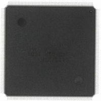
HD6417727F160CV Renesas Electronics America, HD6417727F160CV Datasheet - Page 362

HD6417727F160CV
Manufacturer Part Number
HD6417727F160CV
Description
IC SH MPU ROMLESS 240QFN
Manufacturer
Renesas Electronics America
Series
SuperH® SH7700r
Datasheet
1.HD6417727BP100CV.pdf
(1098 pages)
Specifications of HD6417727F160CV
Core Processor
SH-3 DSP
Core Size
32-Bit
Speed
160MHz
Connectivity
FIFO, SCI, SIO, SmartCard, USB
Peripherals
DMA, LCD, POR, WDT
Number Of I /o
104
Program Memory Type
ROMless
Ram Size
32K x 8
Voltage - Supply (vcc/vdd)
1.7 V ~ 2.05 V
Data Converters
A/D 6x10b; D/A 2x8b
Oscillator Type
Internal
Operating Temperature
-20°C ~ 75°C
Package / Case
240-QFP
Lead Free Status / RoHS Status
Lead free / RoHS Compliant
Eeprom Size
-
Program Memory Size
-
Available stocks
Company
Part Number
Manufacturer
Quantity
Price
Company:
Part Number:
HD6417727F160CV
Manufacturer:
RENESAS
Quantity:
37
Company:
Part Number:
HD6417727F160CV
Manufacturer:
RENESAS
Quantity:
753
- Current page: 362 of 1098
- Download datasheet (7Mb)
Section 12 Bus State Controller (BSC)
Bits 13 and 12—RAS–CAS Delay (RCD1, RCD0): When synchronous DRAM interface is
selected, sets the bank active read/write command delay time.
Bit 13: RCD1
0
1
Bits 11 and 10—Write-Precharge Delay (TRWL1, TRWL0): The TRWL bits set the
synchronous DRAM write-precharge delay time. This designates the time between the end of a
write cycle and the next bank-active command. This is valid only when synchronous DRAM is
connected. After the write cycle, the next bank-active command is not issued for the period TPC +
TRWL.
Bit 11: TRWL1
0
1
Bits 9 and 8—CAS-Before-RAS Refresh RAS Assert Time (TRAS1, TRAS0): When
synchronous DRAM interface is selected, no bank-active command is issues during the period
TPC + TRAS after an auto-refresh command.
Bit 9: TRAS1
0
1
Bit 7—Reserved: This bit is always read as 0. The write value should always be 0.
Bits 6 to 3—Address Multiplex (AMX3 , AMX2, AMX1, AMX0): The AMX bits specify
address multiplexing for synchronous DRAM. The actual address shift value differs between
synchronous DRAM interface.
Rev.6.00 Mar. 27, 2009 Page 304 of 1036
REJ09B0254-0600
Bit 12: RCD0
0
1
0
1
Bit 10: TRWL0
0
1
0
1
Bit 8: TRAS0
0
1
0
1
Description
1 cycle
2 cycles
3 cycles
4 cycles
Description
1 cycle
2 cycles
3 cycles
Reserved (Setting disabled)
Description
2 cycles
3 cycles
4 cycles
5 cycles
(Initial value)
(Initial value)
(Initial value)
Related parts for HD6417727F160CV
Image
Part Number
Description
Manufacturer
Datasheet
Request
R

Part Number:
Description:
KIT STARTER FOR M16C/29
Manufacturer:
Renesas Electronics America
Datasheet:

Part Number:
Description:
KIT STARTER FOR R8C/2D
Manufacturer:
Renesas Electronics America
Datasheet:

Part Number:
Description:
R0K33062P STARTER KIT
Manufacturer:
Renesas Electronics America
Datasheet:

Part Number:
Description:
KIT STARTER FOR R8C/23 E8A
Manufacturer:
Renesas Electronics America
Datasheet:

Part Number:
Description:
KIT STARTER FOR R8C/25
Manufacturer:
Renesas Electronics America
Datasheet:

Part Number:
Description:
KIT STARTER H8S2456 SHARPE DSPLY
Manufacturer:
Renesas Electronics America
Datasheet:

Part Number:
Description:
KIT STARTER FOR R8C38C
Manufacturer:
Renesas Electronics America
Datasheet:

Part Number:
Description:
KIT STARTER FOR R8C35C
Manufacturer:
Renesas Electronics America
Datasheet:

Part Number:
Description:
KIT STARTER FOR R8CL3AC+LCD APPS
Manufacturer:
Renesas Electronics America
Datasheet:

Part Number:
Description:
KIT STARTER FOR RX610
Manufacturer:
Renesas Electronics America
Datasheet:

Part Number:
Description:
KIT STARTER FOR R32C/118
Manufacturer:
Renesas Electronics America
Datasheet:

Part Number:
Description:
KIT DEV RSK-R8C/26-29
Manufacturer:
Renesas Electronics America
Datasheet:

Part Number:
Description:
KIT STARTER FOR SH7124
Manufacturer:
Renesas Electronics America
Datasheet:

Part Number:
Description:
KIT STARTER FOR H8SX/1622
Manufacturer:
Renesas Electronics America
Datasheet:

Part Number:
Description:
KIT DEV FOR SH7203
Manufacturer:
Renesas Electronics America
Datasheet:


