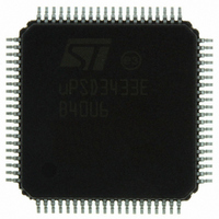
UPSD3433EB40U6 STMicroelectronics, UPSD3433EB40U6 Datasheet - Page 117

UPSD3433EB40U6
Manufacturer Part Number
UPSD3433EB40U6
Description
MCU 8BIT 8032 128KB FLASH 80TQFP
Manufacturer
STMicroelectronics
Series
µPSDr
Datasheet
1.UPSD3434EB40T6.pdf
(293 pages)
Specifications of UPSD3433EB40U6
Core Processor
8032
Core Size
8-Bit
Speed
40MHz
Connectivity
I²C, IrDA, SPI, UART/USART, USB
Peripherals
LVD, POR, PWM, WDT
Number Of I /o
46
Program Memory Size
160KB (160K x 8)
Program Memory Type
FLASH
Ram Size
8K x 8
Voltage - Supply (vcc/vdd)
3 V ~ 5.5 V
Data Converters
A/D 8x10b
Oscillator Type
Internal
Operating Temperature
-40°C ~ 85°C
Package / Case
80-TQFP, 80-VQFP
For Use With
497-5518 - EVAL BOARD RFID READER497-5046 - KIT TOOL FOR ST7/UPSD/STR7 MCU
Lead Free Status / RoHS Status
Lead free / RoHS Compliant
Eeprom Size
-
Other names
497-5660
Available stocks
Company
Part Number
Manufacturer
Quantity
Price
Company:
Part Number:
UPSD3433EB40U6
Manufacturer:
STMicroelectronics
Quantity:
10 000
- Current page: 117 of 293
- Download datasheet (5Mb)
uPSD34xx
23.3
A few things to know related to these transfers:
●
●
●
●
●
●
●
●
Figure 42. Data Transfer on an I
Operating modes
The I
●
●
●
●
Condition
Start
Either the Master or Slave device can hold the SCL clock line low to indicate it needs
more time to handle a byte transfer. An indefinite holding period is possible.
A START condition is generated by a Master and recognized by a Slave when SDA has
a 1-to-0 transition while SCL is high
A STOP condition is generated by a Master and recognized by a Slave when SDA has
a 0-to1 transition while SCL is high
A RE-START (repeated START) condition generated by a Master can have the same
function as a STOP condition when starting another data transfer immediately following
the previous data transfer
When transferring data, the logic level on the SDA line must remain stable while SCL is
high, and SDA can change only while SCL is low. However, when not transferring data,
SDA may change state while SCL is high, which creates the START and STOP bus
conditions.
An Acknowlegde bit is generated from a Master or a Slave by driving SDA low during
the “ninth” bit time, just following each 8-bit byte that is transfered on the bus
on page
bit time. All byte transfers on the I
Acknowlege (ACK) or Non-Acknowledge (NACK).
An additional Master device that desires to control the bus should wait until the bus is
not busy before generating a START condition so that a possible Slave operation is not
interrupted.
If two Master devices both try to generate a START condition simultaneously, the
Master who looses arbitration will switch immediately to Slave mode so it can
recoginize its own Slave address should it appear on the bus.
Master-Transmitter
Master-Receiver
Slave-Transmitter
Slave-Receiver
2
C interface supports four operating modes:
MSB
1
117). A Non-Acknowledge occurs when SDA is asserted high during the ninth
7-bit Slave
2
Address
Clock can be held low
3-6
to stall transfer.
7
READ/WRITE
(Figure 42 on page
Indicator
R/W
8
2
C Bus
2
ACK
C bus include a 9th bit time reserved for an
9
(Figure 42 on page
(Figure 42 on page
MSB
Acknowledge
1
117).
bits from
receiver
Repeated if more
data bytes are
transferred.
2
117).
3-8
117).
ACK
NACK
9
I
2
C interface
(Figure 42
Stop
Condition
Repeated
Start
Condition
117/293
AI09625
Related parts for UPSD3433EB40U6
Image
Part Number
Description
Manufacturer
Datasheet
Request
R

Part Number:
Description:
MCU 8BIT 8032 128KB FLASH 80TQFP
Manufacturer:
STMicroelectronics
Datasheet:

Part Number:
Description:
MCU 8BIT 8032 128KB FLASH 52TQFP
Manufacturer:
STMicroelectronics
Datasheet:

Part Number:
Description:
STMicroelectronics [RIPPLE-CARRY BINARY COUNTER/DIVIDERS]
Manufacturer:
STMicroelectronics
Datasheet:

Part Number:
Description:
STMicroelectronics [LIQUID-CRYSTAL DISPLAY DRIVERS]
Manufacturer:
STMicroelectronics
Datasheet:

Part Number:
Description:
BOARD EVAL FOR MEMS SENSORS
Manufacturer:
STMicroelectronics
Datasheet:

Part Number:
Description:
NPN TRANSISTOR POWER MODULE
Manufacturer:
STMicroelectronics
Datasheet:

Part Number:
Description:
TURBOSWITCH ULTRA-FAST HIGH VOLTAGE DIODE
Manufacturer:
STMicroelectronics
Datasheet:

Part Number:
Description:
Manufacturer:
STMicroelectronics
Datasheet:

Part Number:
Description:
DIODE / SCR MODULE
Manufacturer:
STMicroelectronics
Datasheet:

Part Number:
Description:
DIODE / SCR MODULE
Manufacturer:
STMicroelectronics
Datasheet:

Part Number:
Description:
Search -----> STE16N100
Manufacturer:
STMicroelectronics
Datasheet:

Part Number:
Description:
Search ---> STE53NA50
Manufacturer:
STMicroelectronics
Datasheet:


