UPSD3433EB40U6 STMicroelectronics, UPSD3433EB40U6 Datasheet - Page 210
UPSD3433EB40U6
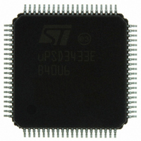
Manufacturer Part Number
UPSD3433EB40U6
Description
MCU 8BIT 8032 128KB FLASH 80TQFP
Manufacturer
STMicroelectronics
Series
µPSDr
Datasheet
1.UPSD3434EB40T6.pdf
(293 pages)
Specifications of UPSD3433EB40U6
Core Processor
8032
Core Size
8-Bit
Speed
40MHz
Connectivity
I²C, IrDA, SPI, UART/USART, USB
Peripherals
LVD, POR, PWM, WDT
Number Of I /o
46
Program Memory Size
160KB (160K x 8)
Program Memory Type
FLASH
Ram Size
8K x 8
Voltage - Supply (vcc/vdd)
3 V ~ 5.5 V
Data Converters
A/D 8x10b
Oscillator Type
Internal
Operating Temperature
-40°C ~ 85°C
Package / Case
80-TQFP, 80-VQFP
For Use With
497-5518 - EVAL BOARD RFID READER497-5046 - KIT TOOL FOR ST7/UPSD/STR7 MCU
Lead Free Status / RoHS Status
Lead free / RoHS Compliant
Eeprom Size
-
Other names
497-5660
Available stocks
Company
Part Number
Manufacturer
Quantity
Price
Company:

Part Number:
UPSD3433EB40U6
Manufacturer:
STMicroelectronics
Quantity:
10 000


PSD module
28.5.16
28.5.17
210/293
Bulk Erase operation are detailed in the section entitled
memory. on page
During a Bulk Erase operation, the Flash memory does not accept any other Flash
instruction sequences.
Flash sector erase
The Sector Erase instruction sequence uses six WRITE operations, as described in
Table 107 on page
same Flash array may be issued by the 8032 if the additional commands are sent within a
limited amount of time.
The Erase Time-out Flag Bit (DQ3) reflects the time-out period allowed between two
consecutive sector erase instruction sequence bytes. If multiple sector erase commands are
desired, the additional sector erase commands (30h) must be sent by the 8032 to another
sector within 80µs after the previous sector erase command. DQ3 is 0 before this time
period has expired, indicating it is OK to issue additional sector erase commands. DQ3 will
go to logic ’1’ if the time has been longer than 80µs since the previous sector erase
command (time has expired), indicating that is not OK to send another sector erase
command. In this case, the 8032 must start a new sector erase instruction sequence (unlock
and command), beginning again after the current sector erase operation has completed.
During a Sector Erase operation, the memory status may be checked by reading the Error
Flag Bit (DQ5), the Toggle Flag Bit (DQ6), and the Data Polling Flag Bit (DQ7), as detailed in
Section 28.5.5: Reading the erase/program status bits on page
During a Sector Erase operation, a Flash memory accepts only Reset Flash and Suspend
Sector Erase instruction sequences. Erasure of one Flash memory sector may be
suspended, in order to read data from another Flash memory sector, and then resumed.
The address provided with the initial Flash Sector Erase command sequence
page
sector erase commands that are appended within the time-out period must be addressed to
other desired segments within the same Flash memory array.
Suspend sector erase
When a Sector Erase operation is in progress, the Suspend Sector Erase instruction
sequence can be used to suspend the operation by writing B0h to any valid address within
the Flash array that currently is undergoing an erase operation. This allows reading of data
from a different Flash memory sector within the same array after the Erase operation has
been suspended. Suspend Sector Erase is accepted only during an Erase operation.
There is up to 15µs delay after the Suspend Sector Erase command is accepted and the
array goes to Read Array mode. The 8032 will monitor the Toggle Flag Bit (DQ6) to
determine when the erase operation has halted and Read Array mode is active.
203) must select the first desired sector (FSx or CSBOOTx) to erase. Subsequent
205.
203. Additional Flash Sector Erase commands to other sectors within the
“Section 28.5.9: Programming Flash
204.
(Table 107 on
uPSD34xx
Related parts for UPSD3433EB40U6
Image
Part Number
Description
Manufacturer
Datasheet
Request
R

Part Number:
Description:
MCU 8BIT 8032 128KB FLASH 80TQFP
Manufacturer:
STMicroelectronics
Datasheet:
Part Number:
Description:
MCU 8BIT 8032 128KB FLASH 52TQFP
Manufacturer:
STMicroelectronics
Datasheet:
Part Number:
Description:
STMicroelectronics [RIPPLE-CARRY BINARY COUNTER/DIVIDERS]
Manufacturer:
STMicroelectronics
Datasheet:
Part Number:
Description:
STMicroelectronics [LIQUID-CRYSTAL DISPLAY DRIVERS]
Manufacturer:
STMicroelectronics
Datasheet:

Part Number:
Description:
BOARD EVAL FOR MEMS SENSORS
Manufacturer:
STMicroelectronics
Datasheet:
Part Number:
Description:
NPN TRANSISTOR POWER MODULE
Manufacturer:
STMicroelectronics
Datasheet:
Part Number:
Description:
TURBOSWITCH ULTRA-FAST HIGH VOLTAGE DIODE
Manufacturer:
STMicroelectronics
Datasheet:
Part Number:
Description:
Manufacturer:
STMicroelectronics
Datasheet:
Part Number:
Description:
DIODE / SCR MODULE
Manufacturer:
STMicroelectronics
Datasheet:
Part Number:
Description:
DIODE / SCR MODULE
Manufacturer:
STMicroelectronics
Datasheet:
Part Number:
Description:
Search -----> STE16N100
Manufacturer:
STMicroelectronics
Datasheet:
Part Number:
Description:
Search ---> STE53NA50
Manufacturer:
STMicroelectronics
Datasheet: