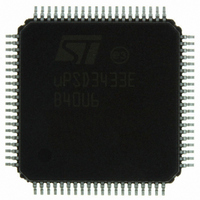
UPSD3433EB40U6 STMicroelectronics, UPSD3433EB40U6 Datasheet - Page 219

UPSD3433EB40U6
Manufacturer Part Number
UPSD3433EB40U6
Description
MCU 8BIT 8032 128KB FLASH 80TQFP
Manufacturer
STMicroelectronics
Series
µPSDr
Datasheet
1.UPSD3434EB40T6.pdf
(293 pages)
Specifications of UPSD3433EB40U6
Core Processor
8032
Core Size
8-Bit
Speed
40MHz
Connectivity
I²C, IrDA, SPI, UART/USART, USB
Peripherals
LVD, POR, PWM, WDT
Number Of I /o
46
Program Memory Size
160KB (160K x 8)
Program Memory Type
FLASH
Ram Size
8K x 8
Voltage - Supply (vcc/vdd)
3 V ~ 5.5 V
Data Converters
A/D 8x10b
Oscillator Type
Internal
Operating Temperature
-40°C ~ 85°C
Package / Case
80-TQFP, 80-VQFP
For Use With
497-5518 - EVAL BOARD RFID READER497-5046 - KIT TOOL FOR ST7/UPSD/STR7 MCU
Lead Free Status / RoHS Status
Lead free / RoHS Compliant
Eeprom Size
-
Other names
497-5660
Available stocks
Company
Part Number
Manufacturer
Quantity
Price
Company:
Part Number:
UPSD3433EB40U6
Manufacturer:
STMicroelectronics
Quantity:
10 000
- Current page: 219 of 293
- Download datasheet (5Mb)
uPSD34xx
28.5.28
Output macrocell
The GPLD has 16 OMCs. Architecture of one individual OMC is shown in
can be used for internal node feedback (buried registers to build shift registers, etc.), or their
outputs may be routed to external port pins. The user can choose any mixture of OMCs
used for buried functions and OMCs used to drive port pins.
Referring to
AND-OR Array to form logic, and also borrowed product terms are available (if unused) from
other OMCs. The polarity of the final product term output is controlled by the XOR gate.
Each OMC can implement sequential logic using the flip-flop element, or combinatorial logic
when bypassing the flip-flop as selected by the output multiplexer. An OMC output can drive
a port pin through the OMC Allocator, it can also drive the 8032 data bus, and also it can
drive a feedback path to the AND-OR Array inputs, all at the same time.
The flip-flop in each OMC can be synthesized as a D, T, JK, or SR type in PSDsoft Express.
OMC flip-flops are specified using PSDsoft Express in the “User Defined Nodes” section of
the Design Assistant. Each flip-flop’s clock, preset, and clear inputs may be driven
individually from a product term of the AND-OR Array, defined by equations in PSDsoft
Express for signals *. c, *.pr, and *.re respectively. The preset and clear inputs on the flip-
flops are level activated, active-high logic signals. The clock inputs on the flip-flops are
rising-edge logic signals.
Optionally, the signal CLKIN (pin PD1) can be used for a common clock source to all OMC
flip-flops. Each flip-flop is clocked on the rising edge. A common clock is specified in
PSDsoft Express by assigning the function “Common Clock Input” for pin PD1 in the Pin
Definition section, and then choosing the signal CLKIN when specifying the clock input (*.c)
for individual flip-flops in the “User Defined Nodes” section.
Figure
77, for each OMC there are native product terms available from the
Figure
PSD module
77. OMCs
219/293
Related parts for UPSD3433EB40U6
Image
Part Number
Description
Manufacturer
Datasheet
Request
R

Part Number:
Description:
MCU 8BIT 8032 128KB FLASH 80TQFP
Manufacturer:
STMicroelectronics
Datasheet:

Part Number:
Description:
MCU 8BIT 8032 128KB FLASH 52TQFP
Manufacturer:
STMicroelectronics
Datasheet:

Part Number:
Description:
STMicroelectronics [RIPPLE-CARRY BINARY COUNTER/DIVIDERS]
Manufacturer:
STMicroelectronics
Datasheet:

Part Number:
Description:
STMicroelectronics [LIQUID-CRYSTAL DISPLAY DRIVERS]
Manufacturer:
STMicroelectronics
Datasheet:

Part Number:
Description:
BOARD EVAL FOR MEMS SENSORS
Manufacturer:
STMicroelectronics
Datasheet:

Part Number:
Description:
NPN TRANSISTOR POWER MODULE
Manufacturer:
STMicroelectronics
Datasheet:

Part Number:
Description:
TURBOSWITCH ULTRA-FAST HIGH VOLTAGE DIODE
Manufacturer:
STMicroelectronics
Datasheet:

Part Number:
Description:
Manufacturer:
STMicroelectronics
Datasheet:

Part Number:
Description:
DIODE / SCR MODULE
Manufacturer:
STMicroelectronics
Datasheet:

Part Number:
Description:
DIODE / SCR MODULE
Manufacturer:
STMicroelectronics
Datasheet:

Part Number:
Description:
Search -----> STE16N100
Manufacturer:
STMicroelectronics
Datasheet:

Part Number:
Description:
Search ---> STE53NA50
Manufacturer:
STMicroelectronics
Datasheet:


