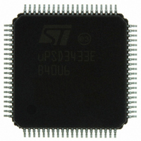
UPSD3433EB40U6 STMicroelectronics, UPSD3433EB40U6 Datasheet - Page 149

UPSD3433EB40U6
Manufacturer Part Number
UPSD3433EB40U6
Description
MCU 8BIT 8032 128KB FLASH 80TQFP
Manufacturer
STMicroelectronics
Series
µPSDr
Datasheet
1.UPSD3434EB40T6.pdf
(293 pages)
Specifications of UPSD3433EB40U6
Core Processor
8032
Core Size
8-Bit
Speed
40MHz
Connectivity
I²C, IrDA, SPI, UART/USART, USB
Peripherals
LVD, POR, PWM, WDT
Number Of I /o
46
Program Memory Size
160KB (160K x 8)
Program Memory Type
FLASH
Ram Size
8K x 8
Voltage - Supply (vcc/vdd)
3 V ~ 5.5 V
Data Converters
A/D 8x10b
Oscillator Type
Internal
Operating Temperature
-40°C ~ 85°C
Package / Case
80-TQFP, 80-VQFP
For Use With
497-5518 - EVAL BOARD RFID READER497-5046 - KIT TOOL FOR ST7/UPSD/STR7 MCU
Lead Free Status / RoHS Status
Lead free / RoHS Compliant
Eeprom Size
-
Other names
497-5660
Available stocks
Company
Part Number
Manufacturer
Quantity
Price
Company:
Part Number:
UPSD3433EB40U6
Manufacturer:
STMicroelectronics
Quantity:
10 000
- Current page: 149 of 293
- Download datasheet (5Mb)
uPSD34xx
25.3
25.3.1
25.3.2
Figure 53. Control transfer
Endpoint FIFOs
The uPSD34xx’s USB module includes 5 endpoints and 10 FIFOs. Each endpoint has two
FIFOs with one for IN and the other for OUT transactions. Each FIFO is 64 bytes long and
is selectively made visible in a 64-byte XDATA segment for CPU access. For efficient data
transfers, the FIFOs may be paired for double buffering. With double buffering, the CPU may
operate on the contents in one buffer while the SIE is transmitting or receiving data in the
paired buffer. uPSD34xx supported endpoints and FIFOs are shown in
Busy Bit (BSY) operation
Each FIFO has a busy bit (BSY) that indicates when the USB SIE has ownership of the
FIFO. When the SIE has ownership of the FIFO, it is either writing data to or reading data
from the FIFO. The SIE writes data to the FIFO when it is receiving an OUT packet and
reads data from the FIFO when it is sending data in response to an IN packet. The CPU is
only permitted to access the FIFO when it is not busy and accesses to it while busy are
ignored. Once the IN FIFO has been written with data by the CPU, the CPU updates the
USIZE register with the number of bytes written to the FIFO. The value written to the USIZE
register tells the SIE the number of bytes to send to the host in response to an IN packet.
Once the USIZE register is written, the FIFOs busy bit is set and remains set until the data
has been transmitted in response to an IN packet. The busy bit for an OUT FIFO is set as
soon as the SIE starts receiving an OUT packet from the host. Once all the data has been
received and written to the FIFO, the SIE clears the busy bit and writes the number of bytes
received to the USIZE register.
Busy bit and interrupts
When the FIFO’s interrupt is enabled, a transition of the busy bit from a '1' to a '0' (when
ownership of the FIFO changes from the SIE to the CPU) generates a USB interrupt with the
corresponding flag set. For an interrupt on an IN FIFO, the CPU must fill the FIFO with the
next set of data to be sent and then update the USIZE register with the number of bytes to
send. For an interrupt on an OUT FIFO, the CPU reads the USIZE register to determine the
number of bytes received and then reads that number of data bytes out of the FIFO.
SETUP ADDR
OUT
IN
ADDR
ADDR
Token Packet
Token Packet
Token Packet
ENDP
ENDP
ENDP
CRC5
CRC5
CRC5
Data0
Data1
Data1
Data Packet
CRC16
Data (8 bytes)
Data Packet
Data Packet
Payload
Payload
Data
Handshake
Packet
ACK
CRC16
CRC16
Handshake Packet
Handshake Packet
ACK
ACK
Table 68
USB interface
(Optional)
STATUS
SETUP
Stage
Stage
Stage
DATA
AI10492
149/293
Related parts for UPSD3433EB40U6
Image
Part Number
Description
Manufacturer
Datasheet
Request
R

Part Number:
Description:
MCU 8BIT 8032 128KB FLASH 80TQFP
Manufacturer:
STMicroelectronics
Datasheet:

Part Number:
Description:
MCU 8BIT 8032 128KB FLASH 52TQFP
Manufacturer:
STMicroelectronics
Datasheet:

Part Number:
Description:
STMicroelectronics [RIPPLE-CARRY BINARY COUNTER/DIVIDERS]
Manufacturer:
STMicroelectronics
Datasheet:

Part Number:
Description:
STMicroelectronics [LIQUID-CRYSTAL DISPLAY DRIVERS]
Manufacturer:
STMicroelectronics
Datasheet:

Part Number:
Description:
BOARD EVAL FOR MEMS SENSORS
Manufacturer:
STMicroelectronics
Datasheet:

Part Number:
Description:
NPN TRANSISTOR POWER MODULE
Manufacturer:
STMicroelectronics
Datasheet:

Part Number:
Description:
TURBOSWITCH ULTRA-FAST HIGH VOLTAGE DIODE
Manufacturer:
STMicroelectronics
Datasheet:

Part Number:
Description:
Manufacturer:
STMicroelectronics
Datasheet:

Part Number:
Description:
DIODE / SCR MODULE
Manufacturer:
STMicroelectronics
Datasheet:

Part Number:
Description:
DIODE / SCR MODULE
Manufacturer:
STMicroelectronics
Datasheet:

Part Number:
Description:
Search -----> STE16N100
Manufacturer:
STMicroelectronics
Datasheet:

Part Number:
Description:
Search ---> STE53NA50
Manufacturer:
STMicroelectronics
Datasheet:


