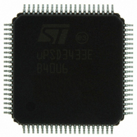
UPSD3433EB40U6 STMicroelectronics, UPSD3433EB40U6 Datasheet - Page 205

UPSD3433EB40U6
Manufacturer Part Number
UPSD3433EB40U6
Description
MCU 8BIT 8032 128KB FLASH 80TQFP
Manufacturer
STMicroelectronics
Series
µPSDr
Datasheet
1.UPSD3434EB40T6.pdf
(293 pages)
Specifications of UPSD3433EB40U6
Core Processor
8032
Core Size
8-Bit
Speed
40MHz
Connectivity
I²C, IrDA, SPI, UART/USART, USB
Peripherals
LVD, POR, PWM, WDT
Number Of I /o
46
Program Memory Size
160KB (160K x 8)
Program Memory Type
FLASH
Ram Size
8K x 8
Voltage - Supply (vcc/vdd)
3 V ~ 5.5 V
Data Converters
A/D 8x10b
Oscillator Type
Internal
Operating Temperature
-40°C ~ 85°C
Package / Case
80-TQFP, 80-VQFP
For Use With
497-5518 - EVAL BOARD RFID READER497-5046 - KIT TOOL FOR ST7/UPSD/STR7 MCU
Lead Free Status / RoHS Status
Lead free / RoHS Compliant
Eeprom Size
-
Other names
497-5660
Available stocks
Company
Part Number
Manufacturer
Quantity
Price
Company:
Part Number:
UPSD3433EB40U6
Manufacturer:
STMicroelectronics
Quantity:
10 000
- Current page: 205 of 293
- Download datasheet (5Mb)
uPSD34xx
28.5.7
28.5.8
28.5.9
Toggle flag (DQ6)
The Flash memories offer an alternate way to determine when a Flash memory program
operation has completed. During the program operation and while the correct sector select
FSx or CSBOOTx is active, the Toggle Flag Bit (DQ6) toggles from '0' to '1' and '1' to ’0’ on
subsequent attempts to read any byte of the same Flash array.
When the internal program operation is complete, the toggling stops and the data read on
the data bus D0-7 is the actual value of the addressed memory byte. The device is now
accessible for a new READ or WRITE operation. The operation is finished when two
successive READs yield the same value for DQ6.
DQ6 may also be used to indicate when an erase operation has completed. During an erase
operation, DQ6 will toggle from '0' to '1' and '1' to ’0’ until the erase operation is complete,
then DQ6 stops toggling. The erase is finished when two successive READs yield the same
value of DQ6. The correct sector select signal, FSx or CSBOOTx, must be active during the
entire procedure.
DQ6 is valid after the fourth instruction byte WRITE operation (for program instruction
sequence) or after the sixth instruction byte WRITE operation (for erase instruction
sequence).
If all the Flash memory sectors selected for erasure are protected, DQ6 toggles to ’0’ for
about 100µs, then returns value of D6 of the previously addressed byte.
Error Flag (DQ5). During a normal program or erase operation, the Error Flag Bit (DQ5) is
to ’0’. This bit is set to ’1’ when there is a failure during Flash memory byte program, sector
erase, or bulk erase operations.
In the case of Flash memory programming, DQ5 Bit indicates an attempt to program a Flash
memory bit from the programmed state of '0,' to the erased state of 1, which is not valid.
DQ5 may also indicate a particular Flash cell is damaged and cannot be programmed.
In case of an error in a Flash memory sector erase or byte program operation, the Flash
memory sector in which the error occurred or to which the programmed byte belongs must
no longer be used. Other Flash memory sectors may still be used. DQ5 is reset after a
Reset Flash instruction sequence.
Erase time-out flag (DQ3)
The Erase Time-out Flag Bit (DQ3) reflects the time-out period allowed between two
consecutive sector erase instruction sequence bytes. If multiple sector erase commands are
desired, the additional sector erase commands (30h) must be sent by the 8032 within 80us
after the previous sector erase command. DQ3 is 0 before this time period has expired,
indicating it is OK to issue additional sector erase commands. DQ3 will go to logic ’1’ if the
time has been longer than 80µs since the previous sector erase command (time has
expired), indication that is not OK to send another sector erase command. In this case, the
8032 must start a new sector erase instruction sequence (unlock and command) beginning
again after the current sector erase operation has completed.
Programming Flash memory.
When a byte of Flash memory is programmed, individual bits are programmed to logic '0.'
cannot program a bit in Flash memory to a logic ’1’ once it has been programmed to a logic
'0.' A bit must be erased to logic ’1’, and programmed to logic '0.' That means Flash memory
must be erased prior to being programmed. A byte of Flash memory is erased to all 1s
PSD module
205/293
Related parts for UPSD3433EB40U6
Image
Part Number
Description
Manufacturer
Datasheet
Request
R

Part Number:
Description:
MCU 8BIT 8032 128KB FLASH 80TQFP
Manufacturer:
STMicroelectronics
Datasheet:

Part Number:
Description:
MCU 8BIT 8032 128KB FLASH 52TQFP
Manufacturer:
STMicroelectronics
Datasheet:

Part Number:
Description:
STMicroelectronics [RIPPLE-CARRY BINARY COUNTER/DIVIDERS]
Manufacturer:
STMicroelectronics
Datasheet:

Part Number:
Description:
STMicroelectronics [LIQUID-CRYSTAL DISPLAY DRIVERS]
Manufacturer:
STMicroelectronics
Datasheet:

Part Number:
Description:
BOARD EVAL FOR MEMS SENSORS
Manufacturer:
STMicroelectronics
Datasheet:

Part Number:
Description:
NPN TRANSISTOR POWER MODULE
Manufacturer:
STMicroelectronics
Datasheet:

Part Number:
Description:
TURBOSWITCH ULTRA-FAST HIGH VOLTAGE DIODE
Manufacturer:
STMicroelectronics
Datasheet:

Part Number:
Description:
Manufacturer:
STMicroelectronics
Datasheet:

Part Number:
Description:
DIODE / SCR MODULE
Manufacturer:
STMicroelectronics
Datasheet:

Part Number:
Description:
DIODE / SCR MODULE
Manufacturer:
STMicroelectronics
Datasheet:

Part Number:
Description:
Search -----> STE16N100
Manufacturer:
STMicroelectronics
Datasheet:

Part Number:
Description:
Search ---> STE53NA50
Manufacturer:
STMicroelectronics
Datasheet:


