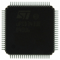
UPSD3433EB40U6 STMicroelectronics, UPSD3433EB40U6 Datasheet - Page 225

UPSD3433EB40U6
Manufacturer Part Number
UPSD3433EB40U6
Description
MCU 8BIT 8032 128KB FLASH 80TQFP
Manufacturer
STMicroelectronics
Series
µPSDr
Datasheet
1.UPSD3434EB40T6.pdf
(293 pages)
Specifications of UPSD3433EB40U6
Core Processor
8032
Core Size
8-Bit
Speed
40MHz
Connectivity
I²C, IrDA, SPI, UART/USART, USB
Peripherals
LVD, POR, PWM, WDT
Number Of I /o
46
Program Memory Size
160KB (160K x 8)
Program Memory Type
FLASH
Ram Size
8K x 8
Voltage - Supply (vcc/vdd)
3 V ~ 5.5 V
Data Converters
A/D 8x10b
Oscillator Type
Internal
Operating Temperature
-40°C ~ 85°C
Package / Case
80-TQFP, 80-VQFP
For Use With
497-5518 - EVAL BOARD RFID READER497-5046 - KIT TOOL FOR ST7/UPSD/STR7 MCU
Lead Free Status / RoHS Status
Lead free / RoHS Compliant
Eeprom Size
-
Other names
497-5660
Available stocks
Company
Part Number
Manufacturer
Quantity
Price
Company:
Part Number:
UPSD3433EB40U6
Manufacturer:
STMicroelectronics
Quantity:
10 000
- Current page: 225 of 293
- Download datasheet (5Mb)
uPSD34xx
28.5.34
28.5.35
28.5.36
I/O ports
There are four programmable I/O ports on the PSD Module: Port A (80-pin device only), Port
B, Port C, and Port D. Ports A and B are eight bits each, Port C is four bits, and Port D is two
bits for 80-pin devices or 1-bit for 52-pin devices. Each port pin is individually configurable,
thus allowing multiple functions per port. The ports are configured using PSDsoft Express
then programming with JTAG, and also by the 8032 writing to csiop registers at run-time.
Topics discussed in this section are:
●
●
●
General port architecture
The general architecture for a single I/O Port pin is shown in
structures for Ports A, B, C, and D differ slightly and are shown in
though
Figure 80 on page 226
value that the 8032 writes to csiop Direction, Drive, Control, and Data Out. The I/O Port logic
contains an output mux whose mux select signal is determined by PSDsoft Express and the
csiop Control register bits at run-time. Inputs to this output mux include the following:
1.
2.
3.
4.
The Port Data Buffer (PDB) provides feedback to the 8032 and allows only one source at a
time to be read when the 8032 reads various csiop registers. There is one PDB for each port
pin enabling the 8032 to read the following on a pin-by-pin basis:
1.
2.
3.
4.
5.
6.
A port pin’s output enable signal is controlled by a two input OR gate whose inputs come
from: a product term of the AND-OR array; the output of the csiop Direction Register. If an
output enable from the AND-OR Array is not defined, and the port pin is not defined as an
OMC output, and if Peripheral I/O mode is not used, then the csiop Direction Register has
sole control of the OE signal.
As shown in
and is also separately routed to an IMC, allowing the 8032 to read a port pin by two different
methods (MCU I/O input mode or read the IMC).
Port operating modes
I/O Port logic has several modes of operation.
modes are available on each port. Each of the port operating modes are described in
General Port architecture
Port Operating Modes
Individual Port Structure
Data from the csiop Data Out register for MCU I/O output mode (All ports)
Latched de-multiplexed 8032 Address for Address Output mode (Ports A and B only)
Peripheral I/O mode data bit (Port A only)
GPLD OMC output (Ports A, B, and C).
MCU I/O signal direction setting (csiop Direction reg)
Pin drive type setting (csiop Drive Select reg)
Latched Addr Out mode setting (csiop Control reg)
MCU I/O pin output setting (csiop Data Out reg)
Output Enable of pin driver (csiop Enable Out reg)
MCU I/O pin input (csiop Data In reg)
Figure 88 on page
Figure 80 on page
shows four csiop registers whose outputs are determined by the
241.
226, a physical port pin is connected to the I/O Port logic
Table 115 on page 223
Figure 80 on page
Figure 85 on page 237
summarizes which
PSD module
226. Port
225/293
Related parts for UPSD3433EB40U6
Image
Part Number
Description
Manufacturer
Datasheet
Request
R

Part Number:
Description:
MCU 8BIT 8032 128KB FLASH 80TQFP
Manufacturer:
STMicroelectronics
Datasheet:

Part Number:
Description:
MCU 8BIT 8032 128KB FLASH 52TQFP
Manufacturer:
STMicroelectronics
Datasheet:

Part Number:
Description:
STMicroelectronics [RIPPLE-CARRY BINARY COUNTER/DIVIDERS]
Manufacturer:
STMicroelectronics
Datasheet:

Part Number:
Description:
STMicroelectronics [LIQUID-CRYSTAL DISPLAY DRIVERS]
Manufacturer:
STMicroelectronics
Datasheet:

Part Number:
Description:
BOARD EVAL FOR MEMS SENSORS
Manufacturer:
STMicroelectronics
Datasheet:

Part Number:
Description:
NPN TRANSISTOR POWER MODULE
Manufacturer:
STMicroelectronics
Datasheet:

Part Number:
Description:
TURBOSWITCH ULTRA-FAST HIGH VOLTAGE DIODE
Manufacturer:
STMicroelectronics
Datasheet:

Part Number:
Description:
Manufacturer:
STMicroelectronics
Datasheet:

Part Number:
Description:
DIODE / SCR MODULE
Manufacturer:
STMicroelectronics
Datasheet:

Part Number:
Description:
DIODE / SCR MODULE
Manufacturer:
STMicroelectronics
Datasheet:

Part Number:
Description:
Search -----> STE16N100
Manufacturer:
STMicroelectronics
Datasheet:

Part Number:
Description:
Search ---> STE53NA50
Manufacturer:
STMicroelectronics
Datasheet:


