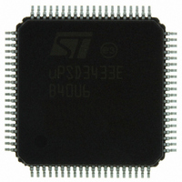
UPSD3433EB40U6 STMicroelectronics, UPSD3433EB40U6 Datasheet - Page 217

UPSD3433EB40U6
Manufacturer Part Number
UPSD3433EB40U6
Description
MCU 8BIT 8032 128KB FLASH 80TQFP
Manufacturer
STMicroelectronics
Series
µPSDr
Datasheet
1.UPSD3434EB40T6.pdf
(293 pages)
Specifications of UPSD3433EB40U6
Core Processor
8032
Core Size
8-Bit
Speed
40MHz
Connectivity
I²C, IrDA, SPI, UART/USART, USB
Peripherals
LVD, POR, PWM, WDT
Number Of I /o
46
Program Memory Size
160KB (160K x 8)
Program Memory Type
FLASH
Ram Size
8K x 8
Voltage - Supply (vcc/vdd)
3 V ~ 5.5 V
Data Converters
A/D 8x10b
Oscillator Type
Internal
Operating Temperature
-40°C ~ 85°C
Package / Case
80-TQFP, 80-VQFP
For Use With
497-5518 - EVAL BOARD RFID READER497-5046 - KIT TOOL FOR ST7/UPSD/STR7 MCU
Lead Free Status / RoHS Status
Lead free / RoHS Compliant
Eeprom Size
-
Other names
497-5660
Available stocks
Company
Part Number
Manufacturer
Quantity
Price
Company:
Part Number:
UPSD3433EB40U6
Manufacturer:
STMicroelectronics
Quantity:
10 000
- Current page: 217 of 293
- Download datasheet (5Mb)
uPSD34xx
28.5.27
Figure 75. DPLD Logic Array
General PLD (GPLD)
The GPLD is used to create general system logic.
architecture of the entire GPLD, and
one OMC, one IMC, and one I/O port pin, which is representative of pins on Ports A, B, and
C. It is important to understand how these elements work together. A more detailed
description will follow for the three major blocks (OMC, IMC, I/O Port) shown in
Figure 76
The GPLD contains:
●
●
●
●
●
●
FLASH MEM PROG STATUS (RDYBSY)
OMC FEEDBACK (MCELLBC.FB0-7)
OMC FEEDBACK (MCELLAB.FB0-7)
AI06601A
POWER-DOWN INDICATOR (PDN)
8032 CNTL (RD, WR, PSEN, ALE)
PIN INPUT PORTS A, B, C (IMCs)
PAGE REGISTER (PGR0 - PGR7)
PSM MODULE RESET (RST)
16 Output Macrocells (OMC)
20 Input Macrocells (IMC)
OMC Allocator
Product Term Allocator inside each OMC
AND-OR Array capable of generating up to 137 product terms
Three I/O Ports, A, B, and C
8032 ADDRESS (A0 - A15)
PIN INPUT PORT D
PLD INPUT BUS
also shows which csiop registers to access for various PLD and I/O functions.
16
20
4
1
1
2
8
8
8
1
Figure 76 on page 218
Figure 74 on page 215
shows the relationship between
PRODUCT TERMS
NUMBER OF
3
3
3
3
3
3
3
3
3
3
3
3
1
1
1
1
2
1
CSBOOT0
CSBOOT1
CSBOOT2
CSBOOT3
shows the
CSIOP
PSEL0
PSEL1
ECS1
ECS0
RS0
FS0
FS1
FS2
FS3
FS4
FS5
FS6
FS7
PSD module
Figure
I/O & CONTROL
REGISTERS
PERIPHERAL
SECONDARY
EXTERNAL
SELECTS
MEMORY
SELECT
SELECTS
SELECT
(PORT D)
SECTOR
I/O MODE
SELECTS
MEMORY
SELECTS
SRAM
FLASH
SECTOR
MAIN
CHIP-
RANGE
FLASH
217/293
76.
Related parts for UPSD3433EB40U6
Image
Part Number
Description
Manufacturer
Datasheet
Request
R

Part Number:
Description:
MCU 8BIT 8032 128KB FLASH 80TQFP
Manufacturer:
STMicroelectronics
Datasheet:

Part Number:
Description:
MCU 8BIT 8032 128KB FLASH 52TQFP
Manufacturer:
STMicroelectronics
Datasheet:

Part Number:
Description:
STMicroelectronics [RIPPLE-CARRY BINARY COUNTER/DIVIDERS]
Manufacturer:
STMicroelectronics
Datasheet:

Part Number:
Description:
STMicroelectronics [LIQUID-CRYSTAL DISPLAY DRIVERS]
Manufacturer:
STMicroelectronics
Datasheet:

Part Number:
Description:
BOARD EVAL FOR MEMS SENSORS
Manufacturer:
STMicroelectronics
Datasheet:

Part Number:
Description:
NPN TRANSISTOR POWER MODULE
Manufacturer:
STMicroelectronics
Datasheet:

Part Number:
Description:
TURBOSWITCH ULTRA-FAST HIGH VOLTAGE DIODE
Manufacturer:
STMicroelectronics
Datasheet:

Part Number:
Description:
Manufacturer:
STMicroelectronics
Datasheet:

Part Number:
Description:
DIODE / SCR MODULE
Manufacturer:
STMicroelectronics
Datasheet:

Part Number:
Description:
DIODE / SCR MODULE
Manufacturer:
STMicroelectronics
Datasheet:

Part Number:
Description:
Search -----> STE16N100
Manufacturer:
STMicroelectronics
Datasheet:

Part Number:
Description:
Search ---> STE53NA50
Manufacturer:
STMicroelectronics
Datasheet:


