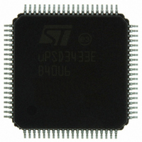
UPSD3433EB40U6 STMicroelectronics, UPSD3433EB40U6 Datasheet - Page 211

UPSD3433EB40U6
Manufacturer Part Number
UPSD3433EB40U6
Description
MCU 8BIT 8032 128KB FLASH 80TQFP
Manufacturer
STMicroelectronics
Series
µPSDr
Datasheet
1.UPSD3434EB40T6.pdf
(293 pages)
Specifications of UPSD3433EB40U6
Core Processor
8032
Core Size
8-Bit
Speed
40MHz
Connectivity
I²C, IrDA, SPI, UART/USART, USB
Peripherals
LVD, POR, PWM, WDT
Number Of I /o
46
Program Memory Size
160KB (160K x 8)
Program Memory Type
FLASH
Ram Size
8K x 8
Voltage - Supply (vcc/vdd)
3 V ~ 5.5 V
Data Converters
A/D 8x10b
Oscillator Type
Internal
Operating Temperature
-40°C ~ 85°C
Package / Case
80-TQFP, 80-VQFP
For Use With
497-5518 - EVAL BOARD RFID READER497-5046 - KIT TOOL FOR ST7/UPSD/STR7 MCU
Lead Free Status / RoHS Status
Lead free / RoHS Compliant
Eeprom Size
-
Other names
497-5660
Available stocks
Company
Part Number
Manufacturer
Quantity
Price
Company:
Part Number:
UPSD3433EB40U6
Manufacturer:
STMicroelectronics
Quantity:
10 000
- Current page: 211 of 293
- Download datasheet (5Mb)
uPSD34xx
28.5.18
28.5.19
28.5.20
28.5.21
If a Suspend Sector Erase instruction sequence was executed, the following rules apply:
●
●
●
●
Resume sector erase
If a Suspend Sector Erase instruction sequence was previously executed, the erase cycle
may be resumed with this instruction sequence. The Resume Sector Erase instruction
sequence consists of writing the command 30h to any valid address within the Flash array
that was suspended as shown in
Reset Flash
The Reset Flash instruction sequence resets the embedded algorithm running on the state
machine in the targeted Flash memory (Main or Secondary) and the memory goes into
Read Array mode. The Reset Flash instruction consists of one bus WRITE cycle as shown
in
occurred during a Flash memory Program or Erase operation.
It may take the Flash memory up to 25µs to complete the Reset cycle. The Reset Flash
instruction sequence is ignored when it is issued during a Program or Bulk Erase operation.
The Reset Flash instruction sequence aborts any on-going Sector Erase operation and
returns the Flash memory to Read Array mode within 25µs.
Reset signal applied to Flash memory
Whenever the PSD Module receives a reset signal from the MCU Module, any operation
that is occurring in either Flash memory array will be aborted and the array(s) will go to
Read Array mode. It may take up to 25µs to abort an operation and achieve Read Array
mode.
A reset from the MCU Module will result from any of these events: an active signal on the
uPSD34xx RESET_IN input pin, a watchdog timer time-out, detection of low V
debug channel reset event.
Flash memory sector protection
Each Flash memory sector can be separately protected against program and erase
operations. This mode can be activated (or deactivated) by selecting this feature in PSDsoft
Express and then programming through the JTAG Port. Sector protection can be selected
for individual sectors, and the 8032 cannot override the protection during run-time. The 8032
can read, but not change, sector protection.
Any attempt to program or erase a protected Flash memory sector is ignored. The 8032 may
read the contents of a Flash sector even when a sector is protected.
Sector protection status is not read using Flash memory instruction sequences, but instead
this status is read by the 8032 reading two registers within csiop address space shown in
Table
Table 107 on page
Attempting to read from a Flash memory sector that was being erased outputs invalid
data.
Reading from a Flash memory sector that was not being erased is valid.
The Flash memory cannot be programmed, and only responds to Resume Sector
Erase and Reset Flash instruction sequences.
If a Reset Flash instruction sequence is received, data in the Flash memory sector that
was being erased is invalid.
109
and Table 110.
203, and it must be executed after any error condition that has
Table 107 on page
203.
CC
PSD module
, or a JTAG
211/293
Related parts for UPSD3433EB40U6
Image
Part Number
Description
Manufacturer
Datasheet
Request
R

Part Number:
Description:
MCU 8BIT 8032 128KB FLASH 80TQFP
Manufacturer:
STMicroelectronics
Datasheet:

Part Number:
Description:
MCU 8BIT 8032 128KB FLASH 52TQFP
Manufacturer:
STMicroelectronics
Datasheet:

Part Number:
Description:
STMicroelectronics [RIPPLE-CARRY BINARY COUNTER/DIVIDERS]
Manufacturer:
STMicroelectronics
Datasheet:

Part Number:
Description:
STMicroelectronics [LIQUID-CRYSTAL DISPLAY DRIVERS]
Manufacturer:
STMicroelectronics
Datasheet:

Part Number:
Description:
BOARD EVAL FOR MEMS SENSORS
Manufacturer:
STMicroelectronics
Datasheet:

Part Number:
Description:
NPN TRANSISTOR POWER MODULE
Manufacturer:
STMicroelectronics
Datasheet:

Part Number:
Description:
TURBOSWITCH ULTRA-FAST HIGH VOLTAGE DIODE
Manufacturer:
STMicroelectronics
Datasheet:

Part Number:
Description:
Manufacturer:
STMicroelectronics
Datasheet:

Part Number:
Description:
DIODE / SCR MODULE
Manufacturer:
STMicroelectronics
Datasheet:

Part Number:
Description:
DIODE / SCR MODULE
Manufacturer:
STMicroelectronics
Datasheet:

Part Number:
Description:
Search -----> STE16N100
Manufacturer:
STMicroelectronics
Datasheet:

Part Number:
Description:
Search ---> STE53NA50
Manufacturer:
STMicroelectronics
Datasheet:


