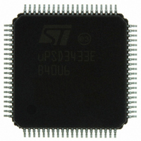
UPSD3433EB40U6 STMicroelectronics, UPSD3433EB40U6 Datasheet - Page 252

UPSD3433EB40U6
Manufacturer Part Number
UPSD3433EB40U6
Description
MCU 8BIT 8032 128KB FLASH 80TQFP
Manufacturer
STMicroelectronics
Series
µPSDr
Datasheet
1.UPSD3434EB40T6.pdf
(293 pages)
Specifications of UPSD3433EB40U6
Core Processor
8032
Core Size
8-Bit
Speed
40MHz
Connectivity
I²C, IrDA, SPI, UART/USART, USB
Peripherals
LVD, POR, PWM, WDT
Number Of I /o
46
Program Memory Size
160KB (160K x 8)
Program Memory Type
FLASH
Ram Size
8K x 8
Voltage - Supply (vcc/vdd)
3 V ~ 5.5 V
Data Converters
A/D 8x10b
Oscillator Type
Internal
Operating Temperature
-40°C ~ 85°C
Package / Case
80-TQFP, 80-VQFP
For Use With
497-5518 - EVAL BOARD RFID READER497-5046 - KIT TOOL FOR ST7/UPSD/STR7 MCU
Lead Free Status / RoHS Status
Lead free / RoHS Compliant
Eeprom Size
-
Other names
497-5660
Available stocks
Company
Part Number
Manufacturer
Quantity
Price
Company:
Part Number:
UPSD3433EB40U6
Manufacturer:
STMicroelectronics
Quantity:
10 000
- Current page: 252 of 293
- Download datasheet (5Mb)
PSD module
28.6.2
252/293
firmware needs to be present for ISP. This is good for manufacturing, for field updates, and
for easy code development in the lab. JTAG-based programmers and debuggers for
uPSD34xx are available from STMicroelectronics and 3rd party vendors.
ISP is different than IAP (In-Application Programming). IAP involves the 8032 to program
Flash memory over any interface supported by the 8032 (e.g., UART, SPI, I2C), which is
good for remote updates over a communication channel. uPSD34xx devices support both
ISP and IAP. The entire PSD Module (Flash memory and PLD) may be programmed with
JTAG ISP, but only the Flash memories may be programmed using IAP.
JTAG chaining inside the package
JTAG protocol allows serial “chaining” of more than one device in a JTAG chain. The
uPSD34xx is assembled with a stacked die process combining the PSD Module (one die)
and the MCU Module (the other die). These two die are chained together within the
uPSD34xx package. The standard JTAG interface has four basic signals:
●
●
●
●
Every device that supports IEEE 1149.1 JTAG communication contains a Test Access Port
(TAP) controller, which is a small state machine to manage JTAG protocol and serial
streams of commands and data. Both the PSD Module and the MCU Module each contain a
TAP controller.
Figure 91
equipment will connect externally to the four IEEE 1149.1 JTAG pins on Port C. The TDI pin
on the uPSD34xx package goes directly to the PSD Module first, then exits the PSD Module
through TDO. TDO of the PSD Module is connected to TDI of the MCU Module. The serial
path is completed when TDO of the MCU Module exits the uPSD34xx package through the
TDO pin on Port C. The JTAG signals TCK and TMS are common to both modules as
specified in IEEE 1149.1. When JTAG devices are chained, typically one devices is in
BYPASS mode while another device is executing a JTAG operation. For the uPSD34xx, the
PSD Module is in BYPASS mode while debugging the MCU Module, and the MCU Module
is in BYPASS mode while performing ISP on the PSD Module.
The RESET_IN input pin on the uPSD34xx package goes to the MCU Module, and this
module will generate the RST reset signal for the PSD Module. These reset signals are
totally independent of the JTAG TAP controllers, meaning that the JTAG channel is
operational when the modules are held in reset. It is required to assert RESET_IN during
ISP. STMicroelectronics and 3rd party JTAG ISP tools will automatically assert a reset signal
during ISP. However, the user must connect this reset signal to RESET_IN as shown in
examples in
TDI - Serial data into device
TDO - Serial data out of device
TCK - Common clock
TMS - Mode Selection
illustrates how these die are chained within a package. JTAG programming/test
Figure 92 on page 254
and
Figure 93 on page
255.
uPSD34xx
Related parts for UPSD3433EB40U6
Image
Part Number
Description
Manufacturer
Datasheet
Request
R

Part Number:
Description:
MCU 8BIT 8032 128KB FLASH 80TQFP
Manufacturer:
STMicroelectronics
Datasheet:

Part Number:
Description:
MCU 8BIT 8032 128KB FLASH 52TQFP
Manufacturer:
STMicroelectronics
Datasheet:

Part Number:
Description:
STMicroelectronics [RIPPLE-CARRY BINARY COUNTER/DIVIDERS]
Manufacturer:
STMicroelectronics
Datasheet:

Part Number:
Description:
STMicroelectronics [LIQUID-CRYSTAL DISPLAY DRIVERS]
Manufacturer:
STMicroelectronics
Datasheet:

Part Number:
Description:
BOARD EVAL FOR MEMS SENSORS
Manufacturer:
STMicroelectronics
Datasheet:

Part Number:
Description:
NPN TRANSISTOR POWER MODULE
Manufacturer:
STMicroelectronics
Datasheet:

Part Number:
Description:
TURBOSWITCH ULTRA-FAST HIGH VOLTAGE DIODE
Manufacturer:
STMicroelectronics
Datasheet:

Part Number:
Description:
Manufacturer:
STMicroelectronics
Datasheet:

Part Number:
Description:
DIODE / SCR MODULE
Manufacturer:
STMicroelectronics
Datasheet:

Part Number:
Description:
DIODE / SCR MODULE
Manufacturer:
STMicroelectronics
Datasheet:

Part Number:
Description:
Search -----> STE16N100
Manufacturer:
STMicroelectronics
Datasheet:

Part Number:
Description:
Search ---> STE53NA50
Manufacturer:
STMicroelectronics
Datasheet:


