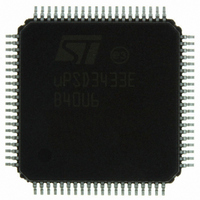
UPSD3433EB40U6 STMicroelectronics, UPSD3433EB40U6 Datasheet - Page 25

UPSD3433EB40U6
Manufacturer Part Number
UPSD3433EB40U6
Description
MCU 8BIT 8032 128KB FLASH 80TQFP
Manufacturer
STMicroelectronics
Series
µPSDr
Datasheet
1.UPSD3434EB40T6.pdf
(293 pages)
Specifications of UPSD3433EB40U6
Core Processor
8032
Core Size
8-Bit
Speed
40MHz
Connectivity
I²C, IrDA, SPI, UART/USART, USB
Peripherals
LVD, POR, PWM, WDT
Number Of I /o
46
Program Memory Size
160KB (160K x 8)
Program Memory Type
FLASH
Ram Size
8K x 8
Voltage - Supply (vcc/vdd)
3 V ~ 5.5 V
Data Converters
A/D 8x10b
Oscillator Type
Internal
Operating Temperature
-40°C ~ 85°C
Package / Case
80-TQFP, 80-VQFP
For Use With
497-5518 - EVAL BOARD RFID READER497-5046 - KIT TOOL FOR ST7/UPSD/STR7 MCU
Lead Free Status / RoHS Status
Lead free / RoHS Compliant
Eeprom Size
-
Other names
497-5660
Available stocks
Company
Part Number
Manufacturer
Quantity
Price
Company:
Part Number:
UPSD3433EB40U6
Manufacturer:
STMicroelectronics
Quantity:
10 000
- Current page: 25 of 293
- Download datasheet (5Mb)
uPSD34xx
5.2
5.3
four MCU clocks). But it is also important to understand PFQ operation on multi-cycle
instructions.
PFQ example, multi-cycle instructions
Let us look at a string of two-byte, two-cycle instructions in
three instructions executed sequentially in this example, instructions A, B, and C. Each of
the time divisions in the figure is one machine-cycle of four clocks, and there are six phases
to reference in this discussion. Each instruction is pre-fetched into the PFQ in advance of
execution by the MCU. Prior to Phase 1, the PFQ has pre-fetched the two instruction bytes
(A1 and A2) of Instruction A. During Phase one, both bytes are loaded into the MCU
execution unit. Also in Phase 1, the PFQ is pre-fetching Instruction B (bytes B1 and B2) from
program memory. In Phase 2, the MCU is processing Instruction A internally while the PFQ
is pre-fetching Instruction C. In Phase 3, both bytes of instruction B are loaded into the MCU
execution unit and the PFQ begins to pre-fetch bytes for the next instruction. In Phase 4
Instruction B is processed.
The uPSD34xx MCU instructions are an exact 1/3 scale of all standard 8032 instructions
with regard to number of cycles per instruction.
instruction sequence from the example above on a standard 8032 for comparison.
Aggregate performance
The stream of two-byte, two-cycle instructions in
5V, uPSD34xx will yield 5 MIPs. And we saw the stream of one- or two-byte, one-cycle
instructions in
will depend on a number of things: the MCU clock frequency; the mixture of instructions
types (bytes and cycles) in the application; the amount of time an empty PFQ stalls the MCU
(mix of instruction types and misses on Branch Cache); and the operating voltage. A 5V
uPSD34xx device operates with four memory wait states, but a 3.3V device operates with
five memory wait states yielding 8 MIPS peak compared to 10 MIPs peak for 5V device. The
same number of wait states will apply to both program fetches and to data READ/WRITEs
unless otherwise specified in the SFR named BUSCON.
In general, a 3X aggregate performance increase is expected over any standard 8032
application running at the same clock frequency.
Figure 9.
PFQ
MCU
Execution
PFQ operation on multi-cycle instructions
Previous Instruction
Figure 7 on page
Inst A, Byte 1&2 Inst B, Byte 1&2 Inst C, Byte 1&2
Macine Cycle
Pre-Fetch
4-clock
Inst A
Three 2-byte, 2-cycle Instructions on uPSD34xx
A1
Phase 1
Pre-Fetch Inst B and C
Instruction A
23, on the same MCU yield 10 MIPs. Effective performance
A2
Process A
Phase 2
8032 MCU core performance enhancements
B1
Next Inst
Phase 3
Figure 10 on page 26
Figure 9 on page
Pre-Fetch next Inst
Instruction B
B2
Process B
Phase 4
Figure 9 on page
Continue to Pre-Fetch
C1
Phase 5
25, running on a 40MHz,
Instruction C
C2
shows the equivalent
Process C
Phase 6
25. There are
Next Inst
AI10432
25/293
Related parts for UPSD3433EB40U6
Image
Part Number
Description
Manufacturer
Datasheet
Request
R

Part Number:
Description:
MCU 8BIT 8032 128KB FLASH 80TQFP
Manufacturer:
STMicroelectronics
Datasheet:

Part Number:
Description:
MCU 8BIT 8032 128KB FLASH 52TQFP
Manufacturer:
STMicroelectronics
Datasheet:

Part Number:
Description:
STMicroelectronics [RIPPLE-CARRY BINARY COUNTER/DIVIDERS]
Manufacturer:
STMicroelectronics
Datasheet:

Part Number:
Description:
STMicroelectronics [LIQUID-CRYSTAL DISPLAY DRIVERS]
Manufacturer:
STMicroelectronics
Datasheet:

Part Number:
Description:
BOARD EVAL FOR MEMS SENSORS
Manufacturer:
STMicroelectronics
Datasheet:

Part Number:
Description:
NPN TRANSISTOR POWER MODULE
Manufacturer:
STMicroelectronics
Datasheet:

Part Number:
Description:
TURBOSWITCH ULTRA-FAST HIGH VOLTAGE DIODE
Manufacturer:
STMicroelectronics
Datasheet:

Part Number:
Description:
Manufacturer:
STMicroelectronics
Datasheet:

Part Number:
Description:
DIODE / SCR MODULE
Manufacturer:
STMicroelectronics
Datasheet:

Part Number:
Description:
DIODE / SCR MODULE
Manufacturer:
STMicroelectronics
Datasheet:

Part Number:
Description:
Search -----> STE16N100
Manufacturer:
STMicroelectronics
Datasheet:

Part Number:
Description:
Search ---> STE53NA50
Manufacturer:
STMicroelectronics
Datasheet:


