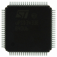
UPSD3433EB40U6 STMicroelectronics, UPSD3433EB40U6 Datasheet - Page 9

UPSD3433EB40U6
Manufacturer Part Number
UPSD3433EB40U6
Description
MCU 8BIT 8032 128KB FLASH 80TQFP
Manufacturer
STMicroelectronics
Series
µPSDr
Datasheet
1.UPSD3434EB40T6.pdf
(293 pages)
Specifications of UPSD3433EB40U6
Core Processor
8032
Core Size
8-Bit
Speed
40MHz
Connectivity
I²C, IrDA, SPI, UART/USART, USB
Peripherals
LVD, POR, PWM, WDT
Number Of I /o
46
Program Memory Size
160KB (160K x 8)
Program Memory Type
FLASH
Ram Size
8K x 8
Voltage - Supply (vcc/vdd)
3 V ~ 5.5 V
Data Converters
A/D 8x10b
Oscillator Type
Internal
Operating Temperature
-40°C ~ 85°C
Package / Case
80-TQFP, 80-VQFP
For Use With
497-5518 - EVAL BOARD RFID READER497-5046 - KIT TOOL FOR ST7/UPSD/STR7 MCU
Lead Free Status / RoHS Status
Lead free / RoHS Compliant
Eeprom Size
-
Other names
497-5660
Available stocks
Company
Part Number
Manufacturer
Quantity
Price
Company:
Part Number:
UPSD3433EB40U6
Manufacturer:
STMicroelectronics
Quantity:
10 000
- Current page: 9 of 293
- Download datasheet (5Mb)
uPSD34xx
1
Note:
Summary description
The Turbo Plus uPSD34xx Series combines a powerful 8051-based microcontroller with a
flexible memory structure, programmable logic, and a rich peripheral mix to form an ideal
embedded controller. At its core is a fast 4-cycle 8032 MCU with a 4-byte instruction
prefetch queue (PFQ) and a 4-entry fully associative branching cache (BC). The MCU is
connected to a 16-bit internal instruction path to maximize performance, enabling loops of
code in smaller localities to execute extremely fast. The 16-bit wide instruction path in the
Turbo Plus Series allows double-byte instructions to be fetched from memory in a single
memory cycle. This keeps the average performance near its peak performance (peak
performance for 5V, 40MHz Turbo Plus uPSD34xx is 10 MIPS for single-byte instructions,
and average performance will be approximately 9 MIPS for mix of single- and multi-byte
instructions).
USB 2.0 (full speed, 12Mbps) is included, providing 10 endpoints, each with its own 64-byte
FIFO to maintain high data throughput. Endpoint 0 (Control Endpoint) uses two of the 10
endpoints for In and Out directions, the remaining eight endpoints may be allocated in any
mix to either type of transfers: Bulk or Interrupt.
Code development is easily managed without a hardware In-Circuit Emulator by using the
serial JTAG debug interface. JTAG is also used for In-System Programming (ISP) in as little
as 10 seconds, perfect for manufacturing and lab development. The 8032 core is coupled to
Programmable System Device (PSD) architecture to optimize the 8032 memory structure,
offering two independent banks of Flash memory that can be placed at virtually any address
within 8032 program or data address space, and easily paged beyond 64K bytes using on-
chip programmable decode logic.
Dual Flash memory banks provide a robust solution for remote product updates in the field
through In-Application Programming (IAP). Dual Flash banks also support EEPROM
emulation, eliminating the need for external EEPROM chips.
General purpose programmable logic (PLD) is included to build an endless variety of glue-
logic, saving external logic devices. The PLD is configured using the software development
tool, PSDsoft Express, available from the web at www.st.com/psm, at no charge.
The uPSD34xx also includes supervisor functions such as a programmable watchdog timer
and low-voltage reset.
For a list of known limitations of the uPSD34xx devices, please refer to
Important
notes.
Summary description
Section 34:
9/293
Related parts for UPSD3433EB40U6
Image
Part Number
Description
Manufacturer
Datasheet
Request
R

Part Number:
Description:
MCU 8BIT 8032 128KB FLASH 80TQFP
Manufacturer:
STMicroelectronics
Datasheet:

Part Number:
Description:
MCU 8BIT 8032 128KB FLASH 52TQFP
Manufacturer:
STMicroelectronics
Datasheet:

Part Number:
Description:
STMicroelectronics [RIPPLE-CARRY BINARY COUNTER/DIVIDERS]
Manufacturer:
STMicroelectronics
Datasheet:

Part Number:
Description:
STMicroelectronics [LIQUID-CRYSTAL DISPLAY DRIVERS]
Manufacturer:
STMicroelectronics
Datasheet:

Part Number:
Description:
BOARD EVAL FOR MEMS SENSORS
Manufacturer:
STMicroelectronics
Datasheet:

Part Number:
Description:
NPN TRANSISTOR POWER MODULE
Manufacturer:
STMicroelectronics
Datasheet:

Part Number:
Description:
TURBOSWITCH ULTRA-FAST HIGH VOLTAGE DIODE
Manufacturer:
STMicroelectronics
Datasheet:

Part Number:
Description:
Manufacturer:
STMicroelectronics
Datasheet:

Part Number:
Description:
DIODE / SCR MODULE
Manufacturer:
STMicroelectronics
Datasheet:

Part Number:
Description:
DIODE / SCR MODULE
Manufacturer:
STMicroelectronics
Datasheet:

Part Number:
Description:
Search -----> STE16N100
Manufacturer:
STMicroelectronics
Datasheet:

Part Number:
Description:
Search ---> STE53NA50
Manufacturer:
STMicroelectronics
Datasheet:


