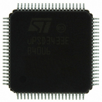
UPSD3433EB40U6 STMicroelectronics, UPSD3433EB40U6 Datasheet - Page 75

UPSD3433EB40U6
Manufacturer Part Number
UPSD3433EB40U6
Description
MCU 8BIT 8032 128KB FLASH 80TQFP
Manufacturer
STMicroelectronics
Series
µPSDr
Datasheet
1.UPSD3434EB40T6.pdf
(293 pages)
Specifications of UPSD3433EB40U6
Core Processor
8032
Core Size
8-Bit
Speed
40MHz
Connectivity
I²C, IrDA, SPI, UART/USART, USB
Peripherals
LVD, POR, PWM, WDT
Number Of I /o
46
Program Memory Size
160KB (160K x 8)
Program Memory Type
FLASH
Ram Size
8K x 8
Voltage - Supply (vcc/vdd)
3 V ~ 5.5 V
Data Converters
A/D 8x10b
Oscillator Type
Internal
Operating Temperature
-40°C ~ 85°C
Package / Case
80-TQFP, 80-VQFP
For Use With
497-5518 - EVAL BOARD RFID READER497-5046 - KIT TOOL FOR ST7/UPSD/STR7 MCU
Lead Free Status / RoHS Status
Lead free / RoHS Compliant
Eeprom Size
-
Other names
497-5660
Available stocks
Company
Part Number
Manufacturer
Quantity
Price
Company:
Part Number:
UPSD3433EB40U6
Manufacturer:
STMicroelectronics
Quantity:
10 000
- Current page: 75 of 293
- Download datasheet (5Mb)
uPSD34xx
outputting a 0-to-1 transition. Only the low-side driver and the internal weak pull-ups are
used. Only Port 3 supports open-drain mode
an external pull-up resistor on each bus signal, typically 4.7KΩ to V
If the alternate function is PCA output, then the related pins are in push-pull mode, meaning
the pins are actively driven and held to logic '1' by the high-side driver, or actively driven and
held to logic '0' by the low-side driver. Only Port 4 supports push-pull mode
page
current when driving logic '0.' This current is significantly more than the capability of pins on
Port 1 or Port 3 (see
For example, to assign these port functions:
●
●
●
The following values need to be written to the SFRs:
Table 30.
Table 31.
Port 3 Pin
P3SFS7
P1SF07
Bit 7
Bit 7
Port 1: UART1, ADC[1:0], P1[7:4] are GPIO
Port 3: UART0, I
Port 4: TCM0, SPI, P4[3:1] are GPIO
P1SFS0 = 00001111b, or 0Fh
P1SFS1 = 00000011b , or 03h
P3SFS = 11000011b, or C3h
P4SFS0 = 11110001b, or F1h
P4SFS1 = 11110000b, or F0h
0
1
2
3
4
5
6
7
72). Port 4 push-pull pins can source I
P3SFS: Port 3 Special Function Select Register (SFR 91h, reset value
00h)
P1SFS0: Port 1 Special Function Select 0 Register (SFR 8Eh, reset value
00h)
P3SFS6
P1SF06
Bit 6
Bit 6
R/W
R,W
R,W
R,W
R,W
R,W
R,W
R,W
R,W
Table 156 on page
2
C, P3[5:2] are GPIO
P3SFS5
P1SF05
P3SFS[i] - 0; Port 3 Pin, i = 0..7
Bit 5
Bit 5
Default Port Function
P3SFS4
P1SF04
GPIO
GPIO
GPIO
GPIO
GPIO
GPIO
GPIO
GPIO
Bit 4
Bit 4
265).
OH
(Figure 18 on page
current when driving logic '1,' and sink I
P3SFS3
P1SF03
Bit 3
Bit 3
P3SFS2
P1SF02
P3SFS[i] - 1; Port 3 Pin, i = 0..7
Bit 2
Bit 2
Alternate Port Function
UART0 Transmit, TXD0
Ext Intr 0/Timer 0 Gate,
Ext Intr 1/Timer 1 Gate,
UART0 Receive, RXD0
72). I
I/O ports of mcu module
Counter 0 Input, C0
Counter 0 Input, C1
I
I
2
CC
2
C Data, I2CSDA
EXT0INT/TG0
EXT1INT/TG1
C Clock, I2CCL
2
.
C requires the use of
P3SFS1
P1SF01
Bit 1
Bit 1
(Figure 19 on
P3SFS0
P1SF00
Bit 0
Bit 0
75/293
OL
Related parts for UPSD3433EB40U6
Image
Part Number
Description
Manufacturer
Datasheet
Request
R

Part Number:
Description:
MCU 8BIT 8032 128KB FLASH 80TQFP
Manufacturer:
STMicroelectronics
Datasheet:

Part Number:
Description:
MCU 8BIT 8032 128KB FLASH 52TQFP
Manufacturer:
STMicroelectronics
Datasheet:

Part Number:
Description:
STMicroelectronics [RIPPLE-CARRY BINARY COUNTER/DIVIDERS]
Manufacturer:
STMicroelectronics
Datasheet:

Part Number:
Description:
STMicroelectronics [LIQUID-CRYSTAL DISPLAY DRIVERS]
Manufacturer:
STMicroelectronics
Datasheet:

Part Number:
Description:
BOARD EVAL FOR MEMS SENSORS
Manufacturer:
STMicroelectronics
Datasheet:

Part Number:
Description:
NPN TRANSISTOR POWER MODULE
Manufacturer:
STMicroelectronics
Datasheet:

Part Number:
Description:
TURBOSWITCH ULTRA-FAST HIGH VOLTAGE DIODE
Manufacturer:
STMicroelectronics
Datasheet:

Part Number:
Description:
Manufacturer:
STMicroelectronics
Datasheet:

Part Number:
Description:
DIODE / SCR MODULE
Manufacturer:
STMicroelectronics
Datasheet:

Part Number:
Description:
DIODE / SCR MODULE
Manufacturer:
STMicroelectronics
Datasheet:

Part Number:
Description:
Search -----> STE16N100
Manufacturer:
STMicroelectronics
Datasheet:

Part Number:
Description:
Search ---> STE53NA50
Manufacturer:
STMicroelectronics
Datasheet:


