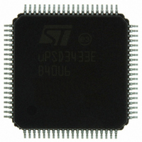
UPSD3433EB40U6 STMicroelectronics, UPSD3433EB40U6 Datasheet - Page 124

UPSD3433EB40U6
Manufacturer Part Number
UPSD3433EB40U6
Description
MCU 8BIT 8032 128KB FLASH 80TQFP
Manufacturer
STMicroelectronics
Series
µPSDr
Datasheet
1.UPSD3434EB40T6.pdf
(293 pages)
Specifications of UPSD3433EB40U6
Core Processor
8032
Core Size
8-Bit
Speed
40MHz
Connectivity
I²C, IrDA, SPI, UART/USART, USB
Peripherals
LVD, POR, PWM, WDT
Number Of I /o
46
Program Memory Size
160KB (160K x 8)
Program Memory Type
FLASH
Ram Size
8K x 8
Voltage - Supply (vcc/vdd)
3 V ~ 5.5 V
Data Converters
A/D 8x10b
Oscillator Type
Internal
Operating Temperature
-40°C ~ 85°C
Package / Case
80-TQFP, 80-VQFP
For Use With
497-5518 - EVAL BOARD RFID READER497-5046 - KIT TOOL FOR ST7/UPSD/STR7 MCU
Lead Free Status / RoHS Status
Lead free / RoHS Compliant
Eeprom Size
-
Other names
497-5660
Available stocks
Company
Part Number
Manufacturer
Quantity
Price
Company:
Part Number:
UPSD3433EB40U6
Manufacturer:
STMicroelectronics
Quantity:
10 000
- Current page: 124 of 293
- Download datasheet (5Mb)
I
23.10
23.10.1
23.11
124/293
2
C interface
I
The S1ADR register
serial byte that has just been received. The MCU may access S1DAT while the SIOE is not
in the process of shifting a byte (the INTR flag indicates shifting is complete).
While transmitting, bytes are shifted out MSB first, and when receiving, bytes are shifted in
MSB first, through the Acknowledge Bit register as shown in
Bus wait condition
After the SIOE finishes receiving a byte in Receive mode, or transmitting a byte in Transmit
mode, the INTR flag (in S1STA) is set and automatically a wait condition is imposed on the
I
as the MCU writes any byte to S1DAT. In Receive mode, the wait condition is released as
soon as the MCU reads the S1DAT register.
This method allows the user to handle transmit and receive operations within an interrupt
service routine. The SIOE will automatically stall the I
the MCU time to get the next byte ready to transmit or time to read the byte that was just
received.
Table 57.
I
The S1ADR register
operating as a Slave. When the SIOE receives an address from a Master, it will compare
this address to the contents of S1ADR, as shown in
If the 7 bits match, the INTR Interrupt flag (in S1STA) is set, and the ADDR Bit (in S1CON) is
set. The SIOE cannot modify the contents S1ADR, and S1ADR is not used during Master
mode.
Table 58.
2
2
2
C bus (SCL held low by SIOE). In Transmit mode, this wait condition is released as soon
C data shift register (S1DAT)
C address register (S1ADR)
SLA6
Bit 7
Bit 7
7:0
7:1
Bit
Bit
0
S1DAT[7:0]
S1DAT: I
S1ADR: I
SLA[6:0]
Symbol
Symbol
SLA5
Bit 6
Bit 6
–
(Table
(Table
2
2
C data shift register (SFR DEh, reset value 00h)
C address register (SFR DFh, reset value 00h)
SLA4
Bit 5
Bit 5
R/W
R/W
R/W
R/W
57) holds a byte of serial data to be transmitted or it holds a
58) holds the 7-bit device address used when the SIOE is
–
Holds the data byte to be transmitted in Transmit mode, or it
holds the data byte received in Receiver mode.
Stores desired 7-bit device address, used when SIOE is in
Slave mode.
Not used
SLA3
Bit 4
Bit 4
S1DAT[7:0]
SLA2
Bit 3
Bit 3
Figure 43 on page
2
C bus at the appropriate time, giving
Function
Function
SLA1
Figure 43 on page
Bit 2
Bit 2
120.
SLA0
Bit 1
Bit 1
120.
uPSD34xx
Bit 0
Bit 0
–
Related parts for UPSD3433EB40U6
Image
Part Number
Description
Manufacturer
Datasheet
Request
R

Part Number:
Description:
MCU 8BIT 8032 128KB FLASH 80TQFP
Manufacturer:
STMicroelectronics
Datasheet:

Part Number:
Description:
MCU 8BIT 8032 128KB FLASH 52TQFP
Manufacturer:
STMicroelectronics
Datasheet:

Part Number:
Description:
STMicroelectronics [RIPPLE-CARRY BINARY COUNTER/DIVIDERS]
Manufacturer:
STMicroelectronics
Datasheet:

Part Number:
Description:
STMicroelectronics [LIQUID-CRYSTAL DISPLAY DRIVERS]
Manufacturer:
STMicroelectronics
Datasheet:

Part Number:
Description:
BOARD EVAL FOR MEMS SENSORS
Manufacturer:
STMicroelectronics
Datasheet:

Part Number:
Description:
NPN TRANSISTOR POWER MODULE
Manufacturer:
STMicroelectronics
Datasheet:

Part Number:
Description:
TURBOSWITCH ULTRA-FAST HIGH VOLTAGE DIODE
Manufacturer:
STMicroelectronics
Datasheet:

Part Number:
Description:
Manufacturer:
STMicroelectronics
Datasheet:

Part Number:
Description:
DIODE / SCR MODULE
Manufacturer:
STMicroelectronics
Datasheet:

Part Number:
Description:
DIODE / SCR MODULE
Manufacturer:
STMicroelectronics
Datasheet:

Part Number:
Description:
Search -----> STE16N100
Manufacturer:
STMicroelectronics
Datasheet:

Part Number:
Description:
Search ---> STE53NA50
Manufacturer:
STMicroelectronics
Datasheet:


