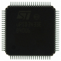
UPSD3433EB40U6 STMicroelectronics, UPSD3433EB40U6 Datasheet - Page 209

UPSD3433EB40U6
Manufacturer Part Number
UPSD3433EB40U6
Description
MCU 8BIT 8032 128KB FLASH 80TQFP
Manufacturer
STMicroelectronics
Series
µPSDr
Datasheet
1.UPSD3434EB40T6.pdf
(293 pages)
Specifications of UPSD3433EB40U6
Core Processor
8032
Core Size
8-Bit
Speed
40MHz
Connectivity
I²C, IrDA, SPI, UART/USART, USB
Peripherals
LVD, POR, PWM, WDT
Number Of I /o
46
Program Memory Size
160KB (160K x 8)
Program Memory Type
FLASH
Ram Size
8K x 8
Voltage - Supply (vcc/vdd)
3 V ~ 5.5 V
Data Converters
A/D 8x10b
Oscillator Type
Internal
Operating Temperature
-40°C ~ 85°C
Package / Case
80-TQFP, 80-VQFP
For Use With
497-5518 - EVAL BOARD RFID READER497-5046 - KIT TOOL FOR ST7/UPSD/STR7 MCU
Lead Free Status / RoHS Status
Lead free / RoHS Compliant
Eeprom Size
-
Other names
497-5660
Available stocks
Company
Part Number
Manufacturer
Quantity
Price
Company:
Part Number:
UPSD3433EB40U6
Manufacturer:
STMicroelectronics
Quantity:
10 000
- Current page: 209 of 293
- Download datasheet (5Mb)
uPSD34xx
28.5.13
28.5.14
28.5.15
indicate when an erase or program operation is complete (requires routing the signal on PC
board from PC3 back into a pin on the MCU Module). This signal is also available internally
on the PSD Module as an input to both PLDs (without routing a signal externally on PC
board) and its signal name is “rd_bsy”. The Ready/Busy output can be probed during lab
development to check the timing of Flash memory programming in the system at run-time.
Bypassed unlock sequence
The Bypass Unlock mode allows the 8032 to program bytes in the Flash memories faster
than using the standard Flash program instruction sequences because the typical AAh, 55h
unlock bus cycles are bypassed for each byte that is programmed. Bypassing the unlock
sequence is typically used when the 8032 is intentionally programming a large number of
bytes (such as during IAP). After intentional programming is complete, typically the Bypass
mode would be disabled, and full protection is back in place to prevent unwanted WRITEs to
Flash memory.
The Bypass Unlock mode is entered by first initiating two Unlock bus cycles. This is followed
by a third WRITE operation containing the Bypass Unlock command, 20h (as shown in
Table 107 on page
the Bypass Unlock mode. After this, a two bus cycle program operation is all that is required
to program a byte in this mode. The first bus cycle in this shortened program instruction
sequence contains the Bypassed Unlocked Program command, A0h, to any valid address
within the unlocked Flash array. The second bus cycle contains the address and data of the
byte to be programmed. Programming status is checked using toggle, polling, or
Ready/Busy just as before. Additional data bytes are programmed the same way until this
Bypass Unlock mode is exited.
To exit Bypass Unlock mode, the system must issue the Reset Bypass Unlock instruction
sequence. The first bus cycle of this instruction must write 90h to any valid address within
the unlocked Flash Array; the second bus cycle must write 00h to any valid address within
the unlocked Flash Array. After this sequence the Flash returns to Read Array mode.
During Bypass Unlock Mode, only the Bypassed Unlock Program instruction, or the Reset
Bypass Unlock instruction is valid, other instruction will be ignored.
Erasing Flash memory
Flash memory may be erased sector-by-sector, or an entire Flash memory array may be
erased with one command (bulk).
Flash bulk erase
The Flash Bulk Erase instruction sequence uses six WRITE operations followed by a READ
operation of the status register, as described in
Bulk Erase instruction sequence is wrong, the Bulk Erase instruction sequence aborts and
the device is reset to the Read Array mode. The address provided by the 8032 during the
Flash Bulk Erase command sequence may select any one of the eight Flash memory sector
select signals FSx or one of the four signals CSBOOTx. An erase of the entire Flash
memory array will occur in a particular array even though a command was sent to just one of
the individual Flash memory sectors within that array.
During a Bulk Erase, the memory status may be checked by reading the Error Flag Bit
(DQ5), the Toggle Flag Bit (DQ6), and the Data Polling Flag Bit (DQ7). The Error Flag Bit
(DQ5) returns a ’1’ if there has been an erase failure. Details of acquiring the status of the
203). The Flash memory array that received that sequence then enters
Table 107 on page
203. If any byte of the
PSD module
209/293
Related parts for UPSD3433EB40U6
Image
Part Number
Description
Manufacturer
Datasheet
Request
R

Part Number:
Description:
MCU 8BIT 8032 128KB FLASH 80TQFP
Manufacturer:
STMicroelectronics
Datasheet:

Part Number:
Description:
MCU 8BIT 8032 128KB FLASH 52TQFP
Manufacturer:
STMicroelectronics
Datasheet:

Part Number:
Description:
STMicroelectronics [RIPPLE-CARRY BINARY COUNTER/DIVIDERS]
Manufacturer:
STMicroelectronics
Datasheet:

Part Number:
Description:
STMicroelectronics [LIQUID-CRYSTAL DISPLAY DRIVERS]
Manufacturer:
STMicroelectronics
Datasheet:

Part Number:
Description:
BOARD EVAL FOR MEMS SENSORS
Manufacturer:
STMicroelectronics
Datasheet:

Part Number:
Description:
NPN TRANSISTOR POWER MODULE
Manufacturer:
STMicroelectronics
Datasheet:

Part Number:
Description:
TURBOSWITCH ULTRA-FAST HIGH VOLTAGE DIODE
Manufacturer:
STMicroelectronics
Datasheet:

Part Number:
Description:
Manufacturer:
STMicroelectronics
Datasheet:

Part Number:
Description:
DIODE / SCR MODULE
Manufacturer:
STMicroelectronics
Datasheet:

Part Number:
Description:
DIODE / SCR MODULE
Manufacturer:
STMicroelectronics
Datasheet:

Part Number:
Description:
Search -----> STE16N100
Manufacturer:
STMicroelectronics
Datasheet:

Part Number:
Description:
Search ---> STE53NA50
Manufacturer:
STMicroelectronics
Datasheet:


