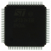
UPSD3433EB40U6 STMicroelectronics, UPSD3433EB40U6 Datasheet - Page 239

UPSD3433EB40U6
Manufacturer Part Number
UPSD3433EB40U6
Description
MCU 8BIT 8032 128KB FLASH 80TQFP
Manufacturer
STMicroelectronics
Series
µPSDr
Datasheet
1.UPSD3434EB40T6.pdf
(293 pages)
Specifications of UPSD3433EB40U6
Core Processor
8032
Core Size
8-Bit
Speed
40MHz
Connectivity
I²C, IrDA, SPI, UART/USART, USB
Peripherals
LVD, POR, PWM, WDT
Number Of I /o
46
Program Memory Size
160KB (160K x 8)
Program Memory Type
FLASH
Ram Size
8K x 8
Voltage - Supply (vcc/vdd)
3 V ~ 5.5 V
Data Converters
A/D 8x10b
Oscillator Type
Internal
Operating Temperature
-40°C ~ 85°C
Package / Case
80-TQFP, 80-VQFP
For Use With
497-5518 - EVAL BOARD RFID READER497-5046 - KIT TOOL FOR ST7/UPSD/STR7 MCU
Lead Free Status / RoHS Status
Lead free / RoHS Compliant
Eeprom Size
-
Other names
497-5660
Available stocks
Company
Part Number
Manufacturer
Quantity
Price
Company:
Part Number:
UPSD3433EB40U6
Manufacturer:
STMicroelectronics
Quantity:
10 000
- Current page: 239 of 293
- Download datasheet (5Mb)
uPSD34xx
Note:
1
2
The remaining four pins (TDI, TDO, TCK, TMS) on Port C are dedicated to the JTAG
function and cannot be used for any other function. See
debug on page
Port C also supports the Open Drain output drive type options on pins PC2, PC3, PC4, and
PC7 using the csiop Drive Select registers.
Figure 87. Port C structure
Pull-up switches to V
Optional function on a specific Port C pin.
if they are used for 6-pin JTAG. See
page 251
–
–
–
FROM AND-
INPUT BUS
ALLOCATOR
FROM OMC
FROM PLD
OR ARRAY
FROM FLASH MEMORIES
PC2 can be used as a voltage input (from battery or other DC source) to backup
the contents of SRAM when V
Express as
PC3 can be used as an output to indicate when a Flash memory program or erase
operation has completed. This is specified in PSDsoft Express as
Ready/Busy (PC3) on page
PC4 can be used as an output to indicate when the SRAM has switched to backup
voltage (when V
in PSDsoft Express as “Standby-On Indicator” (see
standby mode (battery backup) on page
BACK-UP CIRCUIT
STATE MACHINE
TO/FROM JTAG
FROM SRAM
for details.
251.
PT OUTPUT ENABLE, .OE (JTAG STATE MACHINE
AUTOMATICALLY CONTROLS OE FOR JTAG SIGNALS)
PSD MODULE RESET
FROM OMC OUTPUT (MCELLBCx)
DATA
8032
8032 RD
8032
BITS
WR
DATA
8032
BIT
REGIS-
D
CSIOP
TERS
BAT
Section 28.5.62: SRAM standby mode (battery backup) on page
CLR
M
P
D
B
U
X
Q
Q
Q
REGISTERS
1
2
3
4
5
when SRAM goes to battery back-up mode.
ONE of 6
DIRECTION
STANDBY ON
DD
RDY/BSY
TDO, TSTAT
TDI, TMS, TCK
CSIOP
DATA OUT
DIRECTION
DRIVE SELECT
DATA OUT
(MCUI/O)
ENABLE OUT
DATA IN (MCUI/O)
(MCUI/O)
RESET
DRIVE
is less than the battery input voltage on PC2). This is specified
(2)
(2)
(2)
, TERR
208.
(2)
DD
PSDsoft
Section 28.6.1: JTAG ISP and JTAG debug on
1
2
3
4
5
TO IMCs
O
M
U
T
P
U
T
U
X
is lost. This function is specified in PSDsoft
DRIVE TYPE SELECT
OUTPUT
ENABLE
OUTPUT
IMCC2, IMCC3,
250).
IMCC4, IMCC7
PIN
Section 28.6.1: JTAG ISP and JTAG
(2)
NO
HYSTERESIS
Section 28.5.62: SRAM
BUFFER
CMOS
V
DD
V
50k
DD
/V
I/O PORT C
INPUT
BAT
PIN
V
LOGIC
PULL-UP
ONLY ON
JTAG TDI,
TMS, TCK
SIGNALS
DD
(1)
/V
BAT
Section 28.5.12:
TO SRAM
BATTERY
BACK-UP
CIRCUIT
(1)
AI09181
PSD module
TYPICAL
PORT C
PIN,
(2)
239/293
250.
Related parts for UPSD3433EB40U6
Image
Part Number
Description
Manufacturer
Datasheet
Request
R

Part Number:
Description:
MCU 8BIT 8032 128KB FLASH 80TQFP
Manufacturer:
STMicroelectronics
Datasheet:

Part Number:
Description:
MCU 8BIT 8032 128KB FLASH 52TQFP
Manufacturer:
STMicroelectronics
Datasheet:

Part Number:
Description:
STMicroelectronics [RIPPLE-CARRY BINARY COUNTER/DIVIDERS]
Manufacturer:
STMicroelectronics
Datasheet:

Part Number:
Description:
STMicroelectronics [LIQUID-CRYSTAL DISPLAY DRIVERS]
Manufacturer:
STMicroelectronics
Datasheet:

Part Number:
Description:
BOARD EVAL FOR MEMS SENSORS
Manufacturer:
STMicroelectronics
Datasheet:

Part Number:
Description:
NPN TRANSISTOR POWER MODULE
Manufacturer:
STMicroelectronics
Datasheet:

Part Number:
Description:
TURBOSWITCH ULTRA-FAST HIGH VOLTAGE DIODE
Manufacturer:
STMicroelectronics
Datasheet:

Part Number:
Description:
Manufacturer:
STMicroelectronics
Datasheet:

Part Number:
Description:
DIODE / SCR MODULE
Manufacturer:
STMicroelectronics
Datasheet:

Part Number:
Description:
DIODE / SCR MODULE
Manufacturer:
STMicroelectronics
Datasheet:

Part Number:
Description:
Search -----> STE16N100
Manufacturer:
STMicroelectronics
Datasheet:

Part Number:
Description:
Search ---> STE53NA50
Manufacturer:
STMicroelectronics
Datasheet:


