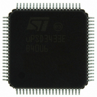
UPSD3433EB40U6 STMicroelectronics, UPSD3433EB40U6 Datasheet - Page 249

UPSD3433EB40U6
Manufacturer Part Number
UPSD3433EB40U6
Description
MCU 8BIT 8032 128KB FLASH 80TQFP
Manufacturer
STMicroelectronics
Series
µPSDr
Datasheet
1.UPSD3434EB40T6.pdf
(293 pages)
Specifications of UPSD3433EB40U6
Core Processor
8032
Core Size
8-Bit
Speed
40MHz
Connectivity
I²C, IrDA, SPI, UART/USART, USB
Peripherals
LVD, POR, PWM, WDT
Number Of I /o
46
Program Memory Size
160KB (160K x 8)
Program Memory Type
FLASH
Ram Size
8K x 8
Voltage - Supply (vcc/vdd)
3 V ~ 5.5 V
Data Converters
A/D 8x10b
Oscillator Type
Internal
Operating Temperature
-40°C ~ 85°C
Package / Case
80-TQFP, 80-VQFP
For Use With
497-5518 - EVAL BOARD RFID READER497-5046 - KIT TOOL FOR ST7/UPSD/STR7 MCU
Lead Free Status / RoHS Status
Lead free / RoHS Compliant
Eeprom Size
-
Other names
497-5660
Available stocks
Company
Part Number
Manufacturer
Quantity
Price
Company:
Part Number:
UPSD3433EB40U6
Manufacturer:
STMicroelectronics
Quantity:
10 000
- Current page: 249 of 293
- Download datasheet (5Mb)
uPSD34xx
28.5.59
28.5.60
28.5.61
of PLD input transitions is zero (no input transitions). Now moving up the frequency axis to
consider the AC current component, current consumption remains considerably less than
Turbo mode until PLD input transitions happen so rapidly that the PLDs do not have time to
latch their outputs and go to standby between the transitions anymore. This is where the
lines converge on the graphs, and current consumption becomes the same for PLD input
transitions at this frequency and higher regardless if Turbo mode is on or off. To determine
the current consumption of the PLDs with Turbo mode off, extrapolate the AC component
from the graph based on number of product terms and input frequency. The only DC
component in non-Turbo mode is the PSD Module standby current.
The key to reducing PLD current consumption is to reduce the composite frequency of
transitions on the PLD input bus, moving down the frequency scale on the graphs. One way
to do this is to carefully select which signals are entering PLD inputs, not selecting high
frequency signals if they are not used in PLD equations. Another way is to use PLD
“Blocking Bits” to block certain signals from entering the PLD input bus.
PLD blocking bits
Blocking specific signals from entering the PLDs using bits of the csiop PMMR registers can
further reduce PLD AC current consumption by lowering the effective composite frequency
of inputs to the PLDs.
Blocking 8032 bus control signals
When the 8032 is active on the MCU Module, four bus control signals (RD, WR, PSEN, and
ALE) are constantly transitioning to manage 8032 bus traffic. Each time one of these signals
has a transition from logic ’1’ to '0,' or 0 to '1,' it will wake up the PLDs if operating in non-
Turbo mode, or when in Turbo mode it will cause the affected PLD gates to draw current. If
equations in the DPLD or GPLD do not use the signals RD, WR, PSEN, or ALE then these
signals can be blocked which will reduce the AC current component substantially. These bus
control signals are rarely used in DPLD equations because they are routed in silicon directly
to the memory arrays of the PSD Module, bypassing the PLDs. For example, it is NOT
necessary to qualify a memory chip select signal with an MCU write strobe, such as “fs0 =
address range & !WR_”. Only “fs0 = address range” is needed.
Each of the 8032 bus control signals may be blocked individually by writing to Bits 2, 3, 4,
and 5 of the PMMR2 register shown in
bus control signals only prevents them from reaching the PLDs, but they will always go to
the memories directly.
However, sometimes it is necessary to use these 8032 bus control signals in the GPLD
when creating interface signals to external I/O peripherals. But it is still possible to save
power by dynamically unblocking the bus signals before reading/writing the external device,
then blocking the signals after the communication is complete.
The user can also block an input signal coming from pin PC7 to the PLD input bus if desired
by writing to Bit 6 of PMMR2.
Blocking common clock, CLKIN
The input CLKIN (from pin PD1) can be blocked to reduce current consumption. CLKIN is
used as a common clock input to all OMC flip-flips, it is a general input to the PLD input bus,
and it is used to clock the APD counter. In PSDsoft Express, the function of pin PD1 must be
Table 145 on page
244. Blocking any of these four
PSD module
249/293
Related parts for UPSD3433EB40U6
Image
Part Number
Description
Manufacturer
Datasheet
Request
R

Part Number:
Description:
MCU 8BIT 8032 128KB FLASH 80TQFP
Manufacturer:
STMicroelectronics
Datasheet:

Part Number:
Description:
MCU 8BIT 8032 128KB FLASH 52TQFP
Manufacturer:
STMicroelectronics
Datasheet:

Part Number:
Description:
STMicroelectronics [RIPPLE-CARRY BINARY COUNTER/DIVIDERS]
Manufacturer:
STMicroelectronics
Datasheet:

Part Number:
Description:
STMicroelectronics [LIQUID-CRYSTAL DISPLAY DRIVERS]
Manufacturer:
STMicroelectronics
Datasheet:

Part Number:
Description:
BOARD EVAL FOR MEMS SENSORS
Manufacturer:
STMicroelectronics
Datasheet:

Part Number:
Description:
NPN TRANSISTOR POWER MODULE
Manufacturer:
STMicroelectronics
Datasheet:

Part Number:
Description:
TURBOSWITCH ULTRA-FAST HIGH VOLTAGE DIODE
Manufacturer:
STMicroelectronics
Datasheet:

Part Number:
Description:
Manufacturer:
STMicroelectronics
Datasheet:

Part Number:
Description:
DIODE / SCR MODULE
Manufacturer:
STMicroelectronics
Datasheet:

Part Number:
Description:
DIODE / SCR MODULE
Manufacturer:
STMicroelectronics
Datasheet:

Part Number:
Description:
Search -----> STE16N100
Manufacturer:
STMicroelectronics
Datasheet:

Part Number:
Description:
Search ---> STE53NA50
Manufacturer:
STMicroelectronics
Datasheet:


