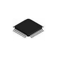
MC68908GZ8MFAE Freescale Semiconductor, MC68908GZ8MFAE Datasheet - Page 144

MC68908GZ8MFAE
Manufacturer Part Number
MC68908GZ8MFAE
Description
IC MCU 8BIT 8K FLASH 48-LQFP
Manufacturer
Freescale Semiconductor
Series
HC08r
Datasheet
1.MC68908GZ8CFJER.pdf
(314 pages)
Specifications of MC68908GZ8MFAE
Core Processor
HC08
Core Size
8-Bit
Speed
8MHz
Connectivity
CAN, LIN, SCI, SPI
Peripherals
LVD, POR, PWM
Number Of I /o
37
Program Memory Size
8KB (8K x 8)
Program Memory Type
FLASH
Ram Size
1K x 8
Voltage - Supply (vcc/vdd)
3 V ~ 5.5 V
Data Converters
A/D 8x10b
Oscillator Type
Internal
Operating Temperature
-40°C ~ 125°C
Package / Case
48-LQFP
Processor Series
M689xx
Core
HC08
Data Bus Width
8 bit
Data Ram Size
1 KB
Interface Type
SPI, SCI, CAN
Maximum Clock Frequency
8 MHz
Number Of Programmable I/os
37
Number Of Timers
2
Operating Supply Voltage
5.5 V
Maximum Operating Temperature
+ 125 C
Mounting Style
SMD/SMT
Development Tools By Supplier
FSICEBASE, M68CBL05AE, DEMO908GZ60E, M68EML08GZE
Minimum Operating Temperature
- 40 C
On-chip Adc
10 bit, 16 Channel
Lead Free Status / RoHS Status
Lead free / RoHS Compliant
Eeprom Size
-
Lead Free Status / Rohs Status
Details
- Current page: 144 of 314
- Download datasheet (5Mb)
MSCAN08 Controller (MSCAN08)
WUPM — Wakeup Mode
CLKSRC — Clock Source
12.13.3 MSCAN08 Bus Timing Register 0
SJW1 and SJW0 — Synchronization Jump Width
BRP5–BRP0 — Baud Rate Prescaler
144
This flag defines whether the integrated low-pass filter is applied to protect the MSCAN08 from
spurious wakeups (see
This flag defines which clock source the MSCAN08 module is driven from (see
The synchronization jump width (SJW) defines the maximum number of time quanta (T
by which a bit may be shortened, or lengthened, to achieve resynchronization on data transitions on
the bus (see
These bits determine the time quanta (T
according to
1 = MSCAN08 will wakeup the CPU only in cases of a dominant pulse on the bus which has a length
0 = MSCAN08 will wakeup the CPU after any recessive-to-dominant edge on the CAN bus.
1 = The MSCAN08 clock source is CGMOUT (see
0 = The MSCAN08 clock source is CGMXCLK/2 (see
of at least t
Address:
The CMCR1 register can be written only if the SFTRES bit in the MSCAN08
module control register is set
Reset:
Table
Read:
Table
Write:
wup
12-7.
12-6).
$0502
SJW1
Bit 7
.
0
12.8.5 Programmable Wakeup
SJW1
Figure 12-18. Bus Timing Register 0 (CBTR0)
MC68HC908GZ16 • MC68HC908GZ8 Data Sheet, Rev. 4
0
0
1
1
Table 12-6. Synchronization Jump Width
SJW0
6
0
BRP5
5
0
q
) clock, which is used to build up the individual bit timing,
NOTE
SJW0
BRP4
4
0
0
1
0
1
Figure
Function).
BRP3
Figure
3
0
12-8).
12-8).
Synchronization
BRP2
Jump Width
2
0
1 T
2 T
3 T
4 T
q
q
q
q
cycle
cycle
cycle
cycle
BRP1
1
0
12.10 Clock
Freescale Semiconductor
BRP0
Bit 0
0
q
) clock cycles
System).
Related parts for MC68908GZ8MFAE
Image
Part Number
Description
Manufacturer
Datasheet
Request
R
Part Number:
Description:
Manufacturer:
Freescale Semiconductor, Inc
Datasheet:
Part Number:
Description:
Manufacturer:
Freescale Semiconductor, Inc
Datasheet:
Part Number:
Description:
Manufacturer:
Freescale Semiconductor, Inc
Datasheet:
Part Number:
Description:
Manufacturer:
Freescale Semiconductor, Inc
Datasheet:
Part Number:
Description:
Manufacturer:
Freescale Semiconductor, Inc
Datasheet:
Part Number:
Description:
Manufacturer:
Freescale Semiconductor, Inc
Datasheet:
Part Number:
Description:
Manufacturer:
Freescale Semiconductor, Inc
Datasheet:
Part Number:
Description:
Manufacturer:
Freescale Semiconductor, Inc
Datasheet:
Part Number:
Description:
Manufacturer:
Freescale Semiconductor, Inc
Datasheet:
Part Number:
Description:
Manufacturer:
Freescale Semiconductor, Inc
Datasheet:
Part Number:
Description:
Manufacturer:
Freescale Semiconductor, Inc
Datasheet:
Part Number:
Description:
Manufacturer:
Freescale Semiconductor, Inc
Datasheet:
Part Number:
Description:
Manufacturer:
Freescale Semiconductor, Inc
Datasheet:
Part Number:
Description:
Manufacturer:
Freescale Semiconductor, Inc
Datasheet:
Part Number:
Description:
Manufacturer:
Freescale Semiconductor, Inc
Datasheet:


