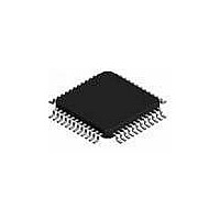
MC68908GZ8MFAE Freescale Semiconductor, MC68908GZ8MFAE Datasheet - Page 50

MC68908GZ8MFAE
Manufacturer Part Number
MC68908GZ8MFAE
Description
IC MCU 8BIT 8K FLASH 48-LQFP
Manufacturer
Freescale Semiconductor
Series
HC08r
Datasheet
1.MC68908GZ8CFJER.pdf
(314 pages)
Specifications of MC68908GZ8MFAE
Core Processor
HC08
Core Size
8-Bit
Speed
8MHz
Connectivity
CAN, LIN, SCI, SPI
Peripherals
LVD, POR, PWM
Number Of I /o
37
Program Memory Size
8KB (8K x 8)
Program Memory Type
FLASH
Ram Size
1K x 8
Voltage - Supply (vcc/vdd)
3 V ~ 5.5 V
Data Converters
A/D 8x10b
Oscillator Type
Internal
Operating Temperature
-40°C ~ 125°C
Package / Case
48-LQFP
Processor Series
M689xx
Core
HC08
Data Bus Width
8 bit
Data Ram Size
1 KB
Interface Type
SPI, SCI, CAN
Maximum Clock Frequency
8 MHz
Number Of Programmable I/os
37
Number Of Timers
2
Operating Supply Voltage
5.5 V
Maximum Operating Temperature
+ 125 C
Mounting Style
SMD/SMT
Development Tools By Supplier
FSICEBASE, M68CBL05AE, DEMO908GZ60E, M68EML08GZE
Minimum Operating Temperature
- 40 C
On-chip Adc
10 bit, 16 Channel
Lead Free Status / RoHS Status
Lead free / RoHS Compliant
Eeprom Size
-
Lead Free Status / Rohs Status
Details
- Current page: 50 of 314
- Download datasheet (5Mb)
Analog-to-Digital Converter (ADC)
3.3.3 Conversion Time
Conversion starts after a write to the ADC status and control register (ADSCR). One conversion will take
between 16 and 17 ADC clock cycles. The ADIVx and ADICLK bits should be set to provide a 1-MHz ADC
clock frequency.
3.3.4 Conversion
In continuous conversion mode, the ADC data register will be filled with new data after each conversion.
Data from the previous conversion will be overwritten whether that data has been read or not.
Conversions will continue until the ADCO bit is cleared. The COCO bit is set after each conversion and
will stay set until the next read of the ADC data register.
In single conversion mode, conversion begins with a write to the ADSCR. Only one conversion occurs
between writes to the ADSCR.
When a conversion is in process and the ADCSCR is written, the current conversion data should be
discarded to prevent an incorrect reading.
3.3.5 Accuracy and Precision
The conversion process is monotonic and has no missing codes.
3.3.6 Result Justification
The conversion result may be formatted in four different ways:
All four of these modes are controlled using MODE0 and MODE1 bits located in the ADC clock register
(ADCLK).
Left justification will place the eight most significant bits (MSB) in the corresponding ADC data register
high, ADRH. This may be useful if the result is to be treated as an 8-bit result where the two least
significant bits (LSB), located in the ADC data register low, ADRL, can be ignored. However, ADRL must
be read after ADRH or else the interlocking will prevent all new conversions from being stored.
Right justification will place only the two MSBs in the corresponding ADC data register high, ADRH, and
the eight LSBs in ADC data register low, ADRL. This mode of operation typically is used when a 10-bit
unsigned result is desired.
Left justified sign data mode is similar to left justified mode with one exception. The MSB of the 10-bit
result, AD9 located in ADRH, is complemented. This mode of operation is useful when a result,
represented as a signed magnitude from mid-scale, is needed. Finally, 8-bit truncation mode will place
the eight MSBs in the ADC data register low, ADRL. The two LSBs are dropped. This mode of operation
50
1. Left justified
2. Right justified
3. Left Justified sign data mode
4. 8-bit truncation mode
Number of bus cycles = conversion time × bus frequency
Conversion time =
MC68HC908GZ16 • MC68HC908GZ8 Data Sheet, Rev. 4
16 to 17 ADC cycles
ADC frequency
Freescale Semiconductor
Related parts for MC68908GZ8MFAE
Image
Part Number
Description
Manufacturer
Datasheet
Request
R
Part Number:
Description:
Manufacturer:
Freescale Semiconductor, Inc
Datasheet:
Part Number:
Description:
Manufacturer:
Freescale Semiconductor, Inc
Datasheet:
Part Number:
Description:
Manufacturer:
Freescale Semiconductor, Inc
Datasheet:
Part Number:
Description:
Manufacturer:
Freescale Semiconductor, Inc
Datasheet:
Part Number:
Description:
Manufacturer:
Freescale Semiconductor, Inc
Datasheet:
Part Number:
Description:
Manufacturer:
Freescale Semiconductor, Inc
Datasheet:
Part Number:
Description:
Manufacturer:
Freescale Semiconductor, Inc
Datasheet:
Part Number:
Description:
Manufacturer:
Freescale Semiconductor, Inc
Datasheet:
Part Number:
Description:
Manufacturer:
Freescale Semiconductor, Inc
Datasheet:
Part Number:
Description:
Manufacturer:
Freescale Semiconductor, Inc
Datasheet:
Part Number:
Description:
Manufacturer:
Freescale Semiconductor, Inc
Datasheet:
Part Number:
Description:
Manufacturer:
Freescale Semiconductor, Inc
Datasheet:
Part Number:
Description:
Manufacturer:
Freescale Semiconductor, Inc
Datasheet:
Part Number:
Description:
Manufacturer:
Freescale Semiconductor, Inc
Datasheet:
Part Number:
Description:
Manufacturer:
Freescale Semiconductor, Inc
Datasheet:


