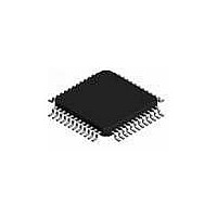
MC68908GZ8MFAE Freescale Semiconductor, MC68908GZ8MFAE Datasheet - Page 71

MC68908GZ8MFAE
Manufacturer Part Number
MC68908GZ8MFAE
Description
IC MCU 8BIT 8K FLASH 48-LQFP
Manufacturer
Freescale Semiconductor
Series
HC08r
Datasheet
1.MC68908GZ8CFJER.pdf
(314 pages)
Specifications of MC68908GZ8MFAE
Core Processor
HC08
Core Size
8-Bit
Speed
8MHz
Connectivity
CAN, LIN, SCI, SPI
Peripherals
LVD, POR, PWM
Number Of I /o
37
Program Memory Size
8KB (8K x 8)
Program Memory Type
FLASH
Ram Size
1K x 8
Voltage - Supply (vcc/vdd)
3 V ~ 5.5 V
Data Converters
A/D 8x10b
Oscillator Type
Internal
Operating Temperature
-40°C ~ 125°C
Package / Case
48-LQFP
Processor Series
M689xx
Core
HC08
Data Bus Width
8 bit
Data Ram Size
1 KB
Interface Type
SPI, SCI, CAN
Maximum Clock Frequency
8 MHz
Number Of Programmable I/os
37
Number Of Timers
2
Operating Supply Voltage
5.5 V
Maximum Operating Temperature
+ 125 C
Mounting Style
SMD/SMT
Development Tools By Supplier
FSICEBASE, M68CBL05AE, DEMO908GZ60E, M68EML08GZE
Minimum Operating Temperature
- 40 C
On-chip Adc
10 bit, 16 Channel
Lead Free Status / RoHS Status
Lead free / RoHS Compliant
Eeprom Size
-
Lead Free Status / Rohs Status
Details
- Current page: 71 of 314
- Download datasheet (5Mb)
VPR1 and VPR0 — VCO Power-of-Two Range Select Bits
4.5.2 PLL Bandwidth Control Register
The PLL bandwidth control register (PBWC):
AUTO — Automatic Bandwidth Control Bit
Freescale Semiconductor
These read/write bits control the VCO’s hardware power-of-two range multiplier E that, in conjunction
with L controls the hardware center-of-range frequency, f
PLLON bit is set. Reset clears these bits. (See
4.5.5 PLL VCO Range Select
•
•
•
•
This read/write bit selects automatic or manual bandwidth control. When initializing the PLL for manual
operation (AUTO = 0), clear the ACQ bit before turning on the PLL. Reset clears the AUTO bit.
1 = Automatic bandwidth control
0 = Manual bandwidth control
Selects automatic or manual (software-controlled) bandwidth control mode
Indicates when the PLL is locked
In automatic bandwidth control mode, indicates when the PLL is in acquisition or tracking mode
In manual operation, forces the PLL into acquisition or tracking mode
Address:
Verify that the value of the VPR1 and VPR0 bits in the PCTL register are
appropriate for the given reference and VCO clock frequencies before
enabling the PLL. See
on selecting the proper value for these control bits.
Reset:
Read:
Write:
1. Do not program E to a value of 3.
$0037
AUTO
Bit 7
Figure 4-5. PLL Bandwidth Control Register (PBWC)
0
VPR1 and VPR0
MC68HC908GZ16 • MC68HC908GZ8 Data Sheet, Rev. 4
Table 4-4. VPR1 and VPR0 Programming
= Unimplemented
00
01
10
LOCK
Register.)
6
0
4.3.6 Programming the PLL
ACQ
5
0
2
NOTE
E
0
1
(1)
4.3.3 PLL
R
4
0
0
= Reserved
VRS
3
0
0
Circuits,
VCO Power-of-Two
Range Multiplier
. VPR1:VPR0 cannot be written when the
for detailed instructions
1
2
4
4.3.6 Programming the
2
0
0
1
0
0
Bit 0
R
0
CGM Registers
PLL, and
71
Related parts for MC68908GZ8MFAE
Image
Part Number
Description
Manufacturer
Datasheet
Request
R
Part Number:
Description:
Manufacturer:
Freescale Semiconductor, Inc
Datasheet:
Part Number:
Description:
Manufacturer:
Freescale Semiconductor, Inc
Datasheet:
Part Number:
Description:
Manufacturer:
Freescale Semiconductor, Inc
Datasheet:
Part Number:
Description:
Manufacturer:
Freescale Semiconductor, Inc
Datasheet:
Part Number:
Description:
Manufacturer:
Freescale Semiconductor, Inc
Datasheet:
Part Number:
Description:
Manufacturer:
Freescale Semiconductor, Inc
Datasheet:
Part Number:
Description:
Manufacturer:
Freescale Semiconductor, Inc
Datasheet:
Part Number:
Description:
Manufacturer:
Freescale Semiconductor, Inc
Datasheet:
Part Number:
Description:
Manufacturer:
Freescale Semiconductor, Inc
Datasheet:
Part Number:
Description:
Manufacturer:
Freescale Semiconductor, Inc
Datasheet:
Part Number:
Description:
Manufacturer:
Freescale Semiconductor, Inc
Datasheet:
Part Number:
Description:
Manufacturer:
Freescale Semiconductor, Inc
Datasheet:
Part Number:
Description:
Manufacturer:
Freescale Semiconductor, Inc
Datasheet:
Part Number:
Description:
Manufacturer:
Freescale Semiconductor, Inc
Datasheet:
Part Number:
Description:
Manufacturer:
Freescale Semiconductor, Inc
Datasheet:


