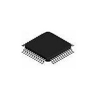
MC68908GZ8MFAE Freescale Semiconductor, MC68908GZ8MFAE Datasheet - Page 57

MC68908GZ8MFAE
Manufacturer Part Number
MC68908GZ8MFAE
Description
IC MCU 8BIT 8K FLASH 48-LQFP
Manufacturer
Freescale Semiconductor
Series
HC08r
Datasheet
1.MC68908GZ8CFJER.pdf
(314 pages)
Specifications of MC68908GZ8MFAE
Core Processor
HC08
Core Size
8-Bit
Speed
8MHz
Connectivity
CAN, LIN, SCI, SPI
Peripherals
LVD, POR, PWM
Number Of I /o
37
Program Memory Size
8KB (8K x 8)
Program Memory Type
FLASH
Ram Size
1K x 8
Voltage - Supply (vcc/vdd)
3 V ~ 5.5 V
Data Converters
A/D 8x10b
Oscillator Type
Internal
Operating Temperature
-40°C ~ 125°C
Package / Case
48-LQFP
Processor Series
M689xx
Core
HC08
Data Bus Width
8 bit
Data Ram Size
1 KB
Interface Type
SPI, SCI, CAN
Maximum Clock Frequency
8 MHz
Number Of Programmable I/os
37
Number Of Timers
2
Operating Supply Voltage
5.5 V
Maximum Operating Temperature
+ 125 C
Mounting Style
SMD/SMT
Development Tools By Supplier
FSICEBASE, M68CBL05AE, DEMO908GZ60E, M68EML08GZE
Minimum Operating Temperature
- 40 C
On-chip Adc
10 bit, 16 Channel
Lead Free Status / RoHS Status
Lead free / RoHS Compliant
Eeprom Size
-
Lead Free Status / Rohs Status
Details
- Current page: 57 of 314
- Download datasheet (5Mb)
3.8.3 ADC Clock Register
The ADC clock register (ADCLK) selects the clock frequency for the ADC.
ADIV2–ADIV0 — ADC Clock Prescaler Bits
ADICLK — ADC Input Clock Select Bit
The ADC requires a clock rate of approximately 1 MHz for correct operation. If the selected clock source
is not fast enough, the ADC will generate incorrect conversions. See
MODE1 and MODE0 — Modes of Result Justification Bits
Freescale Semiconductor
ADIV2–ADIV0 form a 3-bit field which selects the divide ratio used by the ADC to generate the internal
ADC clock.
approximately 1 MHz.
ADICLK selects either the bus clock or the oscillator output clock (CGMXCLK) as the input clock
source to generate the internal ADC clock. Reset selects CGMXCLK as the ADC clock source.
MODE1 and MODE0 select among four modes of operation. The manner in which the ADC conversion
results will be placed in the ADC data registers is controlled by these modes of operation. Reset returns
right-justified mode.
1 = Internal bus clock
0 = Oscillator output clock (CGMXCLK)
00 = 8-bit truncation mode
01 = Right justified mode
10 = Left justified mode
11 = Left justified signed data mode
Address:
Table 3-2
f
ADIC
Reset:
Read:
Write:
=
ADIV2
$003F
Bit 7
1. X = Don’t care
f
CGMXCLK
0
shows the available clock configurations. The ADC clock should be set to
ADIV2
0
0
0
0
1
MC68HC908GZ16 • MC68HC908GZ8 Data Sheet, Rev. 4
Figure 3-9. ADC Clock Register (ADCLK)
= Unimplemented
ADIV1
ADIV[2:0]
6
0
Table 3-2. ADC Clock Divide Ratio
or bus frequency
ADIV1
X
0
0
1
1
(1)
ADIV0
5
0
ADIV0
X
0
1
0
1
(1)
ADICLK
R
4
0
≅ 1 MHz
ADC input clock ÷ 1
ADC input clock ÷ 2
ADC input clock ÷ 4
ADC input clock ÷ 8
ADC input clock ÷ 16
= Reserved
MODE1
3
0
ADC Clock Rate
MODE0
21.10 5.0-Volt ADC
2
1
R
1
0
Bit 0
0
0
Characteristics.
I/O Registers
57
Related parts for MC68908GZ8MFAE
Image
Part Number
Description
Manufacturer
Datasheet
Request
R
Part Number:
Description:
Manufacturer:
Freescale Semiconductor, Inc
Datasheet:
Part Number:
Description:
Manufacturer:
Freescale Semiconductor, Inc
Datasheet:
Part Number:
Description:
Manufacturer:
Freescale Semiconductor, Inc
Datasheet:
Part Number:
Description:
Manufacturer:
Freescale Semiconductor, Inc
Datasheet:
Part Number:
Description:
Manufacturer:
Freescale Semiconductor, Inc
Datasheet:
Part Number:
Description:
Manufacturer:
Freescale Semiconductor, Inc
Datasheet:
Part Number:
Description:
Manufacturer:
Freescale Semiconductor, Inc
Datasheet:
Part Number:
Description:
Manufacturer:
Freescale Semiconductor, Inc
Datasheet:
Part Number:
Description:
Manufacturer:
Freescale Semiconductor, Inc
Datasheet:
Part Number:
Description:
Manufacturer:
Freescale Semiconductor, Inc
Datasheet:
Part Number:
Description:
Manufacturer:
Freescale Semiconductor, Inc
Datasheet:
Part Number:
Description:
Manufacturer:
Freescale Semiconductor, Inc
Datasheet:
Part Number:
Description:
Manufacturer:
Freescale Semiconductor, Inc
Datasheet:
Part Number:
Description:
Manufacturer:
Freescale Semiconductor, Inc
Datasheet:
Part Number:
Description:
Manufacturer:
Freescale Semiconductor, Inc
Datasheet:


