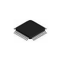
MC68908GZ8MFAE Freescale Semiconductor, MC68908GZ8MFAE Datasheet - Page 290

MC68908GZ8MFAE
Manufacturer Part Number
MC68908GZ8MFAE
Description
IC MCU 8BIT 8K FLASH 48-LQFP
Manufacturer
Freescale Semiconductor
Series
HC08r
Datasheet
1.MC68908GZ8CFJER.pdf
(314 pages)
Specifications of MC68908GZ8MFAE
Core Processor
HC08
Core Size
8-Bit
Speed
8MHz
Connectivity
CAN, LIN, SCI, SPI
Peripherals
LVD, POR, PWM
Number Of I /o
37
Program Memory Size
8KB (8K x 8)
Program Memory Type
FLASH
Ram Size
1K x 8
Voltage - Supply (vcc/vdd)
3 V ~ 5.5 V
Data Converters
A/D 8x10b
Oscillator Type
Internal
Operating Temperature
-40°C ~ 125°C
Package / Case
48-LQFP
Processor Series
M689xx
Core
HC08
Data Bus Width
8 bit
Data Ram Size
1 KB
Interface Type
SPI, SCI, CAN
Maximum Clock Frequency
8 MHz
Number Of Programmable I/os
37
Number Of Timers
2
Operating Supply Voltage
5.5 V
Maximum Operating Temperature
+ 125 C
Mounting Style
SMD/SMT
Development Tools By Supplier
FSICEBASE, M68CBL05AE, DEMO908GZ60E, M68EML08GZE
Minimum Operating Temperature
- 40 C
On-chip Adc
10 bit, 16 Channel
Lead Free Status / RoHS Status
Lead free / RoHS Compliant
Eeprom Size
-
Lead Free Status / Rohs Status
Details
- Current page: 290 of 314
- Download datasheet (5Mb)
Electrical Specifications
290
Monitor mode entry voltage
Low-voltage inhibit, trip falling voltage
Low-voltage inhibit, trip rising voltage
Low-voltage inhibit reset/recover hysteresis
POR rearm voltage
POR reset voltage
POR rise time ramp rate
10. Power supply must maintain regulation within operating V
11. Pullups and pulldowns are disabled. Port B leakage is specified in
12. Maximum is highest voltage that POR is guaranteed.
13. Maximum is highest voltage that POR is possible.
14. If minimum V
1. V
2. Typical values reflect average measurements at midpoint of voltage range, 25°C only.
3. Run (operating) I
4. Wait I
5. Stop I
6. Stop I
7. This parameter is characterized and not tested on each device.
8. All functional non-supply pins are internally clamped to V
9. Input must be current limited to the value specified. To determine the value of the required current-limiting resistor,
(V
loads. Less than 100 pF on all outputs. C
affects run I
than 100 pF on all outputs. C
I
configured as inputs. Typical values at midpoint of voltage range, 25°C only.
rail. No dc loads. Less than 100 pF on all outputs. All inputs configured as inputs.
calculate resistance values for positive and negative clamp voltages, then use the larger of the two values.
conditions. If positive injection current (V
result in external power supply going out of regulation. Ensure external V
injection current. This will be the greatest risk when the MCU is not consuming power. Examples are: if no system clock
is present, or if clock rate is very low (which would reduce overall power consumption).
V
TRIPF
DD
DD
DD
. Measured with CGM and LVI enabled.
= 5.0 Vdc ± 10%, V
is reached.
DD
DD
DD
+ V
measured using external square wave clock source (f
with TBM enabled is measured using an external square wave clock source (f
is measured with OSC1 = V
HYS
DD
DD
= V
(13)
. Measured with all modules enabled.
(12)
is not reached before the internal POR reset is released, RST must be driven low externally until minimum
Characteristic
DD
TRIPR
measured using external square wave clock source (f
(14)
)
SS
= 0 Vdc, T
MC68HC908GZ16 • MC68HC908GZ8 Data Sheet, Rev. 4
L
= 20 pF on OSC2. All ports configured as inputs. OSC2 capacitance linearly affects wait
(1)
SS
A
. All inputs 0.2 V from rail. No dc loads. Less than 100 pF on all outputs. All ports
= T
in
L
> V
A
= 20 pF on OSC2. All ports configured as inputs. OSC2 capacitance linearly
(min) to T
DD
) is greater than I
A
(max), unless otherwise noted
SS
DD
V
Symbol
V
V
and V
PORRST
range during instantaneous and operating maximum current
R
V
V
V
TRIPR
TRIPF
OSC
POR
POR
HYS
TST
DD
= 32 MHz). All inputs 0.2 V from rail. No dc loads. Less
DD
21.10 5.0-Volt ADC
, the injection current may flow out of V
.
DD
V
OSC
DD
0.035
load will shunt current greater than maximum
3.90
4.20
Min
—
0
0
+ 2.5
= 32 MHz). All inputs 0.2 V from rail. No dc
OSC
Characteristics.
Typ
4.25
4.35
100
700
= 8 MHz). All inputs 0.2 V from
—
—
—
(2)
Freescale Semiconductor
V
DD
Max
4.50
4.60
100
800
—
—
+ 4.0
DD
and could
V/ms
Unit
mV
mV
mV
V
V
V
Related parts for MC68908GZ8MFAE
Image
Part Number
Description
Manufacturer
Datasheet
Request
R
Part Number:
Description:
Manufacturer:
Freescale Semiconductor, Inc
Datasheet:
Part Number:
Description:
Manufacturer:
Freescale Semiconductor, Inc
Datasheet:
Part Number:
Description:
Manufacturer:
Freescale Semiconductor, Inc
Datasheet:
Part Number:
Description:
Manufacturer:
Freescale Semiconductor, Inc
Datasheet:
Part Number:
Description:
Manufacturer:
Freescale Semiconductor, Inc
Datasheet:
Part Number:
Description:
Manufacturer:
Freescale Semiconductor, Inc
Datasheet:
Part Number:
Description:
Manufacturer:
Freescale Semiconductor, Inc
Datasheet:
Part Number:
Description:
Manufacturer:
Freescale Semiconductor, Inc
Datasheet:
Part Number:
Description:
Manufacturer:
Freescale Semiconductor, Inc
Datasheet:
Part Number:
Description:
Manufacturer:
Freescale Semiconductor, Inc
Datasheet:
Part Number:
Description:
Manufacturer:
Freescale Semiconductor, Inc
Datasheet:
Part Number:
Description:
Manufacturer:
Freescale Semiconductor, Inc
Datasheet:
Part Number:
Description:
Manufacturer:
Freescale Semiconductor, Inc
Datasheet:
Part Number:
Description:
Manufacturer:
Freescale Semiconductor, Inc
Datasheet:
Part Number:
Description:
Manufacturer:
Freescale Semiconductor, Inc
Datasheet:


