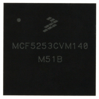
MCF5253CVM140 Freescale Semiconductor, MCF5253CVM140 Datasheet - Page 110

MCF5253CVM140
Manufacturer Part Number
MCF5253CVM140
Description
IC MPU 32BIT 140MHZ 225-MAPBGA
Manufacturer
Freescale Semiconductor
Series
MCF525xr
Datasheets
1.MCF5253VM140J.pdf
(34 pages)
2.MCF5253VM140J.pdf
(8 pages)
3.MCF5253VM140J.pdf
(648 pages)
4.MCF5253VM140J.pdf
(2 pages)
Specifications of MCF5253CVM140
Core Processor
Coldfire V2
Core Size
32-Bit
Speed
140MHz
Connectivity
CAN, EBI/EMI, I²C, QSPI, UART/USART, USB OTG
Peripherals
DMA, WDT
Program Memory Type
ROMless
Ram Size
128K x 8
Voltage - Supply (vcc/vdd)
1.08 V ~ 1.32 V
Data Converters
A/D 6x12b
Oscillator Type
External
Operating Temperature
-40°C ~ 85°C
Package / Case
225-MAPBGA
Family Name
MCF5xxx
Device Core
ColdFire V2
Device Core Size
32b
Frequency (max)
140MHz
Instruction Set Architecture
RISC
Supply Voltage 1 (typ)
1.2/3.3V
Operating Supply Voltage (max)
1.32/3.6V
Operating Supply Voltage (min)
1.08/3V
Operating Temp Range
-40C to 85C
Operating Temperature Classification
Industrial
Mounting
Surface Mount
Pin Count
225
Package Type
MA-BGA
Lead Free Status / RoHS Status
Lead free / RoHS Compliant
Number Of I /o
-
Eeprom Size
-
Program Memory Size
-
Lead Free Status / Rohs Status
Compliant
Available stocks
Company
Part Number
Manufacturer
Quantity
Price
Company:
Part Number:
MCF5253CVM140
Manufacturer:
FREESCALE
Quantity:
300
Company:
Part Number:
MCF5253CVM140
Manufacturer:
Freescale Semiconductor
Quantity:
10 000
Part Number:
MCF5253CVM140
Manufacturer:
FREESCALE
Quantity:
20 000
Company:
Part Number:
MCF5253CVM140J
Manufacturer:
Freescale Semiconductor
Quantity:
10 000
- MCF5253VM140J PDF datasheet
- MCF5253VM140J PDF datasheet #2
- MCF5253VM140J PDF datasheet #3
- MCF5253VM140J PDF datasheet #4
- Current page: 110 of 648
- Download datasheet (8Mb)
Synchronous DRAM Controller Module
7-6
13–12
CASL
IMRS
Field
10–8
CBM
RE
15
14
11
7
6
Table 7-5. DRAM Address and Control Register (DACR0) Field Descriptions (Synchronous Mode)
Refresh enable. Determines when the DRAM controller generates a refresh cycle to the DRAM block.
0 Do not refresh associated DRAM block
1 Refresh associated DRAM block
Reserved, should be cleared.
CAS latency. Affects the following SDRAM timing specifications. Timing nomenclature varies with manufacturers.
Refer to the SDRAM specification for the appropriate timing nomenclature:
Note: The SDRAM controller only supports CAS latencies of 1 or 2. However very few SDRAM devices are available
that support CASL = 1. So we recommend to only use CASL = 2. Some fast SDRAM are now becoming available
and require a CASL = 3 which is not supported by this SDRAM controller.
Reserved, should be cleared.
Command (AP) and Bank Select MUX [2:0]. Because different SDRAM configurations cause the command and bank
select lines to correspond to different addresses, these resources are programmable. CBM determines the
addresses onto which these functions are multiplexed.
CBM Command Bit Bank Select Lines
000 17 18 and up
001 18 19 and up
010 19 20 and up
011 20 21 and up
100 21 22 and up
101 22 23 and up
110 23 24 and up
111 24 25 and up
This encoding and the address multiplexing scheme handle common SDRAM organizations. Bank select lines
include a base line and all address lines above for SDRAMs with multiple bank select lines.
Reserved, should be cleared.
Initiate mode register set (
initialization, IMRS should be set only after all DRAM controller registers are initialized and
commands have been issued. After IMRS is set, the next access to an SDRAM block programs the SDRAM’s mode
register. Thus, the address of the access should be programmed to place the correct mode information on the
SDRAM address pins. Because the SDRAM does not register this information, it doesn’t matter if the IMRS access
is a read or a write. The DRAM controller clears IMRS after the
0 Take no action
1 Initiate
t
t
t
t
t
t
RCD
CASL
RAS
RP
RWL
EP
—Last data out to precharge command)
—Precharge command to ACTV command
MRS
—
—SRAS assertion to SCAS assertion
,
—SCAS assertion to data out
t
RDL
ACTV
command
—Last data input to precharge command
command to precharge command
MRS
Parameter
) command. Setting IMRS generates a
MCF5253 Reference Manual, Rev. 1
(continued)
Description
CASL = 00 CASL = 01 CASL = 10 CASL = 11
N/A
N/A
N/A
N/A
N/A
N/A
MRS
command finishes.
MRS
Number of Bus Clocks
command to the associated SDRAM. In
2
1
4
2
1
1
3
2
6
3
1
1
Freescale Semiconductor
PALL
and
3
2
6
3
1
1
REFRESH
Related parts for MCF5253CVM140
Image
Part Number
Description
Manufacturer
Datasheet
Request
R
Part Number:
Description:
Mcf5253 Coldfire? Microprocessor Data Sheet
Manufacturer:
Freescale Semiconductor, Inc
Datasheet:
Part Number:
Description:
Manufacturer:
Freescale Semiconductor, Inc
Datasheet:
Part Number:
Description:
Manufacturer:
Freescale Semiconductor, Inc
Datasheet:
Part Number:
Description:
Manufacturer:
Freescale Semiconductor, Inc
Datasheet:
Part Number:
Description:
Manufacturer:
Freescale Semiconductor, Inc
Datasheet:
Part Number:
Description:
Manufacturer:
Freescale Semiconductor, Inc
Datasheet:
Part Number:
Description:
Manufacturer:
Freescale Semiconductor, Inc
Datasheet:
Part Number:
Description:
Manufacturer:
Freescale Semiconductor, Inc
Datasheet:
Part Number:
Description:
Manufacturer:
Freescale Semiconductor, Inc
Datasheet:
Part Number:
Description:
Manufacturer:
Freescale Semiconductor, Inc
Datasheet:
Part Number:
Description:
Manufacturer:
Freescale Semiconductor, Inc
Datasheet:
Part Number:
Description:
Manufacturer:
Freescale Semiconductor, Inc
Datasheet:
Part Number:
Description:
Manufacturer:
Freescale Semiconductor, Inc
Datasheet:
Part Number:
Description:
Manufacturer:
Freescale Semiconductor, Inc
Datasheet:
Part Number:
Description:
Manufacturer:
Freescale Semiconductor, Inc
Datasheet:


