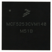
MCF5253CVM140 Freescale Semiconductor, MCF5253CVM140 Datasheet - Page 206

MCF5253CVM140
Manufacturer Part Number
MCF5253CVM140
Description
IC MPU 32BIT 140MHZ 225-MAPBGA
Manufacturer
Freescale Semiconductor
Series
MCF525xr
Datasheets
1.MCF5253VM140J.pdf
(34 pages)
2.MCF5253VM140J.pdf
(8 pages)
3.MCF5253VM140J.pdf
(648 pages)
4.MCF5253VM140J.pdf
(2 pages)
Specifications of MCF5253CVM140
Core Processor
Coldfire V2
Core Size
32-Bit
Speed
140MHz
Connectivity
CAN, EBI/EMI, I²C, QSPI, UART/USART, USB OTG
Peripherals
DMA, WDT
Program Memory Type
ROMless
Ram Size
128K x 8
Voltage - Supply (vcc/vdd)
1.08 V ~ 1.32 V
Data Converters
A/D 6x12b
Oscillator Type
External
Operating Temperature
-40°C ~ 85°C
Package / Case
225-MAPBGA
Family Name
MCF5xxx
Device Core
ColdFire V2
Device Core Size
32b
Frequency (max)
140MHz
Instruction Set Architecture
RISC
Supply Voltage 1 (typ)
1.2/3.3V
Operating Supply Voltage (max)
1.32/3.6V
Operating Supply Voltage (min)
1.08/3V
Operating Temp Range
-40C to 85C
Operating Temperature Classification
Industrial
Mounting
Surface Mount
Pin Count
225
Package Type
MA-BGA
Lead Free Status / RoHS Status
Lead free / RoHS Compliant
Number Of I /o
-
Eeprom Size
-
Program Memory Size
-
Lead Free Status / Rohs Status
Compliant
Available stocks
Company
Part Number
Manufacturer
Quantity
Price
Company:
Part Number:
MCF5253CVM140
Manufacturer:
FREESCALE
Quantity:
300
Company:
Part Number:
MCF5253CVM140
Manufacturer:
Freescale Semiconductor
Quantity:
10 000
Part Number:
MCF5253CVM140
Manufacturer:
FREESCALE
Quantity:
20 000
Company:
Part Number:
MCF5253CVM140J
Manufacturer:
Freescale Semiconductor
Quantity:
10 000
- MCF5253VM140J PDF datasheet
- MCF5253VM140J PDF datasheet #2
- MCF5253VM140J PDF datasheet #3
- MCF5253VM140J PDF datasheet #4
- Current page: 206 of 648
- Download datasheet (8Mb)
IDE and Flash Media Interface
To set up the SmartMedia interface perform the following tasks.
13.2.1
13-8
SmartMedia
tCLS, tCLH,
tALS, tALH
1. Program the three Chip Select registers inside the chip select modules (CSAR2, CSMR2, CSCR2)
2. Program the IDE config1 register. Only fields CS2PRE, CS2POST, BUFEN1CS2EN,
3. Program the IDE config2 register as follows:
Symbol
Timing
as follows:
— CSCR2 bit fields must be programmed as follows:
BUFEN2CS2EN. The values required for the buffer enable signals BUFEN1CS2EN and
BUFEN2CS2EN depend on the hardware configuration. If two buffers are used in cascade, both
bits must be 1. Fields CS2PRE and CS2POST are relevant and are detailed later in this section.
— TA enable 2 = ‘1.’
— IDE_IORDY enable 2 = ‘0.’
— WAITCOUNT2 is required and is explained later in this section.
– AA—0 (TA signal generated by IDEconfig2 register logic)
– WS[3:0]—not relevant
– PS[1:0]—01 (8 bit port size)
– BSTR, BSTW—00 (no burst read/write cycles)
SmartMedia Timing
A SmartMedia interface and an IDE interface cannot be implemented
simultaneously in the same hardware application as they both share the
same read and write strobe signals on the MCF5253.
Typical Value
20, 40
nS
Write data
BUFENB
Address
DIOW
BufEnb
SWE
Clk
Controlled by
Table 13-6. SmartMedia Timing Values
Setting
Figure 13-6. SmartMedia Timing
MCF5253 Reference Manual, Rev. 1
–
t11
Equation (Approximately)
NOTE
CS2PRE > t1 - tbuf
t12
t13
Realized in software because CLE
and ALE are driven by gpio.
Freescale Semiconductor
Comment
Related parts for MCF5253CVM140
Image
Part Number
Description
Manufacturer
Datasheet
Request
R
Part Number:
Description:
Mcf5253 Coldfire? Microprocessor Data Sheet
Manufacturer:
Freescale Semiconductor, Inc
Datasheet:
Part Number:
Description:
Manufacturer:
Freescale Semiconductor, Inc
Datasheet:
Part Number:
Description:
Manufacturer:
Freescale Semiconductor, Inc
Datasheet:
Part Number:
Description:
Manufacturer:
Freescale Semiconductor, Inc
Datasheet:
Part Number:
Description:
Manufacturer:
Freescale Semiconductor, Inc
Datasheet:
Part Number:
Description:
Manufacturer:
Freescale Semiconductor, Inc
Datasheet:
Part Number:
Description:
Manufacturer:
Freescale Semiconductor, Inc
Datasheet:
Part Number:
Description:
Manufacturer:
Freescale Semiconductor, Inc
Datasheet:
Part Number:
Description:
Manufacturer:
Freescale Semiconductor, Inc
Datasheet:
Part Number:
Description:
Manufacturer:
Freescale Semiconductor, Inc
Datasheet:
Part Number:
Description:
Manufacturer:
Freescale Semiconductor, Inc
Datasheet:
Part Number:
Description:
Manufacturer:
Freescale Semiconductor, Inc
Datasheet:
Part Number:
Description:
Manufacturer:
Freescale Semiconductor, Inc
Datasheet:
Part Number:
Description:
Manufacturer:
Freescale Semiconductor, Inc
Datasheet:
Part Number:
Description:
Manufacturer:
Freescale Semiconductor, Inc
Datasheet:


