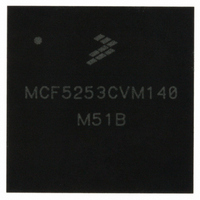
MCF5253CVM140 Freescale Semiconductor, MCF5253CVM140 Datasheet - Page 414

MCF5253CVM140
Manufacturer Part Number
MCF5253CVM140
Description
IC MPU 32BIT 140MHZ 225-MAPBGA
Manufacturer
Freescale Semiconductor
Series
MCF525xr
Datasheets
1.MCF5253VM140J.pdf
(34 pages)
2.MCF5253VM140J.pdf
(8 pages)
3.MCF5253VM140J.pdf
(648 pages)
4.MCF5253VM140J.pdf
(2 pages)
Specifications of MCF5253CVM140
Core Processor
Coldfire V2
Core Size
32-Bit
Speed
140MHz
Connectivity
CAN, EBI/EMI, I²C, QSPI, UART/USART, USB OTG
Peripherals
DMA, WDT
Program Memory Type
ROMless
Ram Size
128K x 8
Voltage - Supply (vcc/vdd)
1.08 V ~ 1.32 V
Data Converters
A/D 6x12b
Oscillator Type
External
Operating Temperature
-40°C ~ 85°C
Package / Case
225-MAPBGA
Family Name
MCF5xxx
Device Core
ColdFire V2
Device Core Size
32b
Frequency (max)
140MHz
Instruction Set Architecture
RISC
Supply Voltage 1 (typ)
1.2/3.3V
Operating Supply Voltage (max)
1.32/3.6V
Operating Supply Voltage (min)
1.08/3V
Operating Temp Range
-40C to 85C
Operating Temperature Classification
Industrial
Mounting
Surface Mount
Pin Count
225
Package Type
MA-BGA
Lead Free Status / RoHS Status
Lead free / RoHS Compliant
Number Of I /o
-
Eeprom Size
-
Program Memory Size
-
Lead Free Status / Rohs Status
Compliant
Available stocks
Company
Part Number
Manufacturer
Quantity
Price
Company:
Part Number:
MCF5253CVM140
Manufacturer:
FREESCALE
Quantity:
300
Company:
Part Number:
MCF5253CVM140
Manufacturer:
Freescale Semiconductor
Quantity:
10 000
Part Number:
MCF5253CVM140
Manufacturer:
FREESCALE
Quantity:
20 000
Company:
Part Number:
MCF5253CVM140J
Manufacturer:
Freescale Semiconductor
Quantity:
10 000
- MCF5253VM140J PDF datasheet
- MCF5253VM140J PDF datasheet #2
- MCF5253VM140J PDF datasheet #3
- MCF5253VM140J PDF datasheet #4
- Current page: 414 of 648
- Download datasheet (8Mb)
IEEE 1149.1 Test Access Port (JTAG)
instruction operations occur. TMS has an internal pullup so that if it is not driven low, its value will default
to a logic level of 1. However, if TMS will not be used, it should be tied to Vdd. This pin also signals a
hardware breakpoint to the processor when in the debug mode.
21.3.4
This is a dual-function pin. If TEST[2:0] = 001, then DSI is selected. If TEST[2:0] = 000, then TDI is
selected. When used as TDI, this input signal provides the serial data port for loading the various JTAG
shift registers composed of the boundary scan register, the bypass register, and the instruction register.
Shifting in of data depends on the state of the JTAG controller state machine and the instruction currently
in the instruction register. This data shift occurs on the rising edge of TCK. TDI also has an internal pullup
so that if it is not driven low its value will default to a logic level of 1. However, if TDI will not be used,
it should be tied to VDD.
This pin also provides the single-bit communication for the debug module commands.
21.3.5
This is a dual-function pin. When TEST[2:0] = 001, then DSO is selected. When TEST[2:0] = 000, TDO
is selected. When used as TDO, this output signal provides the serial data port for outputting data from the
JTAG logic. Shifting out of data depends on the state of the JTAG controller state machine and the
instruction currently in the instruction register. This data shift occurs on the falling edge of TCK. When
TDO is not outputting test data, it is tri-stated. TDO can also be placed in tri-state mode to allow bussed
or parallel connections to other devices having JTAG.
21.4
The state of TMS at the rising edge of TCK determines the current state of the TAP controller. There are
basically two paths that the TAP controller can follow: The first, for executing JTAG instructions; the
second, for manipulating JTAG data based on the JTAG instructions. The various states of the TAP
controller are shown in
JTAG document.
21-4
TAP Controller
Test Data Input/Development Serial Input (TDI/DSI)
Test Data Output/Development Serial Output (TDO/DSO)
From any state that the TAP controller is in, Test-Logic-Reset can be entered
if TMS is held high for at least five rising edges of TCK.
Figure
21-2. For more detail on each state, refer to the IEEE 1149.1A Standard
MCF5253 Reference Manual, Rev. 1
NOTE
Freescale Semiconductor
Related parts for MCF5253CVM140
Image
Part Number
Description
Manufacturer
Datasheet
Request
R
Part Number:
Description:
Mcf5253 Coldfire? Microprocessor Data Sheet
Manufacturer:
Freescale Semiconductor, Inc
Datasheet:
Part Number:
Description:
Manufacturer:
Freescale Semiconductor, Inc
Datasheet:
Part Number:
Description:
Manufacturer:
Freescale Semiconductor, Inc
Datasheet:
Part Number:
Description:
Manufacturer:
Freescale Semiconductor, Inc
Datasheet:
Part Number:
Description:
Manufacturer:
Freescale Semiconductor, Inc
Datasheet:
Part Number:
Description:
Manufacturer:
Freescale Semiconductor, Inc
Datasheet:
Part Number:
Description:
Manufacturer:
Freescale Semiconductor, Inc
Datasheet:
Part Number:
Description:
Manufacturer:
Freescale Semiconductor, Inc
Datasheet:
Part Number:
Description:
Manufacturer:
Freescale Semiconductor, Inc
Datasheet:
Part Number:
Description:
Manufacturer:
Freescale Semiconductor, Inc
Datasheet:
Part Number:
Description:
Manufacturer:
Freescale Semiconductor, Inc
Datasheet:
Part Number:
Description:
Manufacturer:
Freescale Semiconductor, Inc
Datasheet:
Part Number:
Description:
Manufacturer:
Freescale Semiconductor, Inc
Datasheet:
Part Number:
Description:
Manufacturer:
Freescale Semiconductor, Inc
Datasheet:
Part Number:
Description:
Manufacturer:
Freescale Semiconductor, Inc
Datasheet:


