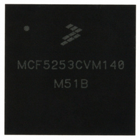
MCF5253CVM140 Freescale Semiconductor, MCF5253CVM140 Datasheet - Page 381

MCF5253CVM140
Manufacturer Part Number
MCF5253CVM140
Description
IC MPU 32BIT 140MHZ 225-MAPBGA
Manufacturer
Freescale Semiconductor
Series
MCF525xr
Datasheets
1.MCF5253VM140J.pdf
(34 pages)
2.MCF5253VM140J.pdf
(8 pages)
3.MCF5253VM140J.pdf
(648 pages)
4.MCF5253VM140J.pdf
(2 pages)
Specifications of MCF5253CVM140
Core Processor
Coldfire V2
Core Size
32-Bit
Speed
140MHz
Connectivity
CAN, EBI/EMI, I²C, QSPI, UART/USART, USB OTG
Peripherals
DMA, WDT
Program Memory Type
ROMless
Ram Size
128K x 8
Voltage - Supply (vcc/vdd)
1.08 V ~ 1.32 V
Data Converters
A/D 6x12b
Oscillator Type
External
Operating Temperature
-40°C ~ 85°C
Package / Case
225-MAPBGA
Family Name
MCF5xxx
Device Core
ColdFire V2
Device Core Size
32b
Frequency (max)
140MHz
Instruction Set Architecture
RISC
Supply Voltage 1 (typ)
1.2/3.3V
Operating Supply Voltage (max)
1.32/3.6V
Operating Supply Voltage (min)
1.08/3V
Operating Temp Range
-40C to 85C
Operating Temperature Classification
Industrial
Mounting
Surface Mount
Pin Count
225
Package Type
MA-BGA
Lead Free Status / RoHS Status
Lead free / RoHS Compliant
Number Of I /o
-
Eeprom Size
-
Program Memory Size
-
Lead Free Status / Rohs Status
Compliant
Available stocks
Company
Part Number
Manufacturer
Quantity
Price
Company:
Part Number:
MCF5253CVM140
Manufacturer:
FREESCALE
Quantity:
300
Company:
Part Number:
MCF5253CVM140
Manufacturer:
Freescale Semiconductor
Quantity:
10 000
Part Number:
MCF5253CVM140
Manufacturer:
FREESCALE
Quantity:
20 000
Company:
Part Number:
MCF5253CVM140J
Manufacturer:
Freescale Semiconductor
Quantity:
10 000
- MCF5253VM140J PDF datasheet
- MCF5253VM140J PDF datasheet #2
- MCF5253VM140J PDF datasheet #3
- MCF5253VM140J PDF datasheet #4
- Current page: 381 of 648
- Download datasheet (8Mb)
1
All ColdFire Family BDM commands include a 16-bit operation word followed by an optional set of one
or more extension words as shown in
Table 20-6
Freescale Semiconductor
Address/Data (A/D) The A/D field is used in commands that operate on address and data registers in the processor. It
Extension Word(s)
General command effect and/or requirements on CPU operation:
Operand Size
(as required)
Halted—The CPU must be halted to perform this command
Steal—Command generates bus cycles which can be interleaved with CPU accesses
Parallel—Command is executed in parallel with CPU activity
Refer to command summaries for detailed operation descriptions.
Operation
Register
Field
R/W
describes the BDM fields.
The operation field specifies the command.
The R/W field specifies the direction of operand transfer. When the bit is set, the transfer is from the CPU
to the development system. When the bit is cleared, data is written to the CPU or to memory from the
development system.
For sized operations, this field specifies the operand data size. All addresses are expressed as 32-bit
absolute values. The size field is encoded as listed in
determines whether the register field specifies a data or address register. A one indicates an address
register; zero, a data register.
In commands that operate on processor registers, this field specifies which register is selected. The field
value contains the register number.
Certain commands require extension words for addresses and/or immediate data. Addresses require two
extension words because only absolute long addressing is permitted. Immediate data can be either one
or two words in length—byte and word data each require a single extension word; longword data requires
two words. Both operands and addresses are transferred most significant word first. In the following
descriptions of the BDM command set, the optional set of extension words is defined as “Address,” “Data,”
or “Operand Data.”
15
14
Table 20-6. BDM Command Register Field Descriptions
OPERATION
13
Encoding
12
00
01
10
11
Figure 20-6. BDM Command Register
Table 20-7. BDM Size Field Encoding
MCF5253 Reference Manual, Rev. 1
11
Table
10
20-6.
EXTENSION WORD(S)
9
0
Operand Size
Longword
Reserved
R/W
8
Word
Byte
OP SIZE
7
Description
6
Table 20-7
5
0
Bit Values
4
0
16 bits
32 bits
8 bits
A/D
3
.
Background Debug Mode (BDM) Interface
2
REGISTER
1
0
20-11
Related parts for MCF5253CVM140
Image
Part Number
Description
Manufacturer
Datasheet
Request
R
Part Number:
Description:
Mcf5253 Coldfire? Microprocessor Data Sheet
Manufacturer:
Freescale Semiconductor, Inc
Datasheet:
Part Number:
Description:
Manufacturer:
Freescale Semiconductor, Inc
Datasheet:
Part Number:
Description:
Manufacturer:
Freescale Semiconductor, Inc
Datasheet:
Part Number:
Description:
Manufacturer:
Freescale Semiconductor, Inc
Datasheet:
Part Number:
Description:
Manufacturer:
Freescale Semiconductor, Inc
Datasheet:
Part Number:
Description:
Manufacturer:
Freescale Semiconductor, Inc
Datasheet:
Part Number:
Description:
Manufacturer:
Freescale Semiconductor, Inc
Datasheet:
Part Number:
Description:
Manufacturer:
Freescale Semiconductor, Inc
Datasheet:
Part Number:
Description:
Manufacturer:
Freescale Semiconductor, Inc
Datasheet:
Part Number:
Description:
Manufacturer:
Freescale Semiconductor, Inc
Datasheet:
Part Number:
Description:
Manufacturer:
Freescale Semiconductor, Inc
Datasheet:
Part Number:
Description:
Manufacturer:
Freescale Semiconductor, Inc
Datasheet:
Part Number:
Description:
Manufacturer:
Freescale Semiconductor, Inc
Datasheet:
Part Number:
Description:
Manufacturer:
Freescale Semiconductor, Inc
Datasheet:
Part Number:
Description:
Manufacturer:
Freescale Semiconductor, Inc
Datasheet:


