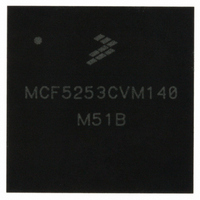
MCF5253CVM140 Freescale Semiconductor, MCF5253CVM140 Datasheet - Page 454

MCF5253CVM140
Manufacturer Part Number
MCF5253CVM140
Description
IC MPU 32BIT 140MHZ 225-MAPBGA
Manufacturer
Freescale Semiconductor
Series
MCF525xr
Datasheets
1.MCF5253VM140J.pdf
(34 pages)
2.MCF5253VM140J.pdf
(8 pages)
3.MCF5253VM140J.pdf
(648 pages)
4.MCF5253VM140J.pdf
(2 pages)
Specifications of MCF5253CVM140
Core Processor
Coldfire V2
Core Size
32-Bit
Speed
140MHz
Connectivity
CAN, EBI/EMI, I²C, QSPI, UART/USART, USB OTG
Peripherals
DMA, WDT
Program Memory Type
ROMless
Ram Size
128K x 8
Voltage - Supply (vcc/vdd)
1.08 V ~ 1.32 V
Data Converters
A/D 6x12b
Oscillator Type
External
Operating Temperature
-40°C ~ 85°C
Package / Case
225-MAPBGA
Family Name
MCF5xxx
Device Core
ColdFire V2
Device Core Size
32b
Frequency (max)
140MHz
Instruction Set Architecture
RISC
Supply Voltage 1 (typ)
1.2/3.3V
Operating Supply Voltage (max)
1.32/3.6V
Operating Supply Voltage (min)
1.08/3V
Operating Temp Range
-40C to 85C
Operating Temperature Classification
Industrial
Mounting
Surface Mount
Pin Count
225
Package Type
MA-BGA
Lead Free Status / RoHS Status
Lead free / RoHS Compliant
Number Of I /o
-
Eeprom Size
-
Program Memory Size
-
Lead Free Status / Rohs Status
Compliant
Available stocks
Company
Part Number
Manufacturer
Quantity
Price
Company:
Part Number:
MCF5253CVM140
Manufacturer:
FREESCALE
Quantity:
300
Company:
Part Number:
MCF5253CVM140
Manufacturer:
Freescale Semiconductor
Quantity:
10 000
Part Number:
MCF5253CVM140
Manufacturer:
FREESCALE
Quantity:
20 000
Company:
Part Number:
MCF5253CVM140J
Manufacturer:
Freescale Semiconductor
Quantity:
10 000
- MCF5253VM140J PDF datasheet
- MCF5253VM140J PDF datasheet #2
- MCF5253VM140J PDF datasheet #3
- MCF5253VM140J PDF datasheet #4
- Current page: 454 of 648
- Download datasheet (8Mb)
Advanced Technology Attachment Controller (ATA)
23.5.2.5
A group of three registers control the interrupt interface from the ATA module and going to the CPU and
DMA. There are two interrupts controlled by these registers:
23-28
Address MBAR2 + 0x824 (ATA_CONTROL)
dma_ultra_selected
Reset
dma_pending
fifo_rcv_en
dma_write
fifo_tx_en
ata_rst_b
fifo_rst_b
iordy_en
W
R
Field
7
6
5
4
3
2
1
0
fifo_rst_b
0
7
Interrupt Registers
This field controls if the internal FIFO is in reset or enabled.
0 FIFO reset
1 FIFO normal operation
This bit controls the level on the ata_reset_b pin, and controls the reset of the internal ata protocol engine.
0 ata_reset_b = 0, ata drive is reset, and internal protocol engine reset.
1 ata_reset_b = 1, ata drive is not reset and internal protocol engine normal operation.
FIFO transmit enable. This bit controls if the FIFO will make transmit data requests to the DMA. If enabled,
the FIFO will request the DMA to refill it whenever FIFO filling drops below the alarm level.
0 FIFO refill by DMA disabled
1 FIFO refill by DMA enabled
FIFO receive enable. This bit controls if the FIFO will make receive data requests to the DMA. If enabled,
the FIFO will request the DMA to empty it whenever FIFO filling becomes greater or equal to the alarm
level.
0 FIFO empty by DMA disabled
1 FIFO empty by DMA enabled
DMA pending bit. This bit controls if the ATA interface will respond to a DMA request originating in the
drive. If this bit is asserted, the ATA interface will start a multiword DMA or ultra DMA burst whenever the
drive asserts ATA_DMARQ.
0 ATA interface will not start DMA burst
1 ATA interface will start multiword DMA or ultra DMA burst whenever drive asserts dmarq
This bit indicates if a DMA burst started, the UDMA or MDMA protocol will be used.
0 Multiword DMA protocol will be used
1 Ultra DMA protocol will be used
This bit indicates the data direction on any DMA burst started.
0 DMA in burst, ATA interface reads from drive
1 DMA out burst, ATA interface writes to drive
This bit indicates if the ATA_IORDY handshake will be used during PIO mode.
0 IORDY will be disregarded
1 IORDY handshake will be used
ata_rst_b
0
6
Table 23-10. ATA Control Register Field Descriptions
fifo_tx_en
0
5
Figure 23-39. ATA_Control Register
MCF5253 Reference Manual, Rev. 1
fifo_rcv_en
0
4
dma_pending
Description
0
3
dma_ultra_selected
0
2
Freescale Semiconductor
Access: User read/write
dma_write
1
0
iordy_en
0
0
Related parts for MCF5253CVM140
Image
Part Number
Description
Manufacturer
Datasheet
Request
R
Part Number:
Description:
Mcf5253 Coldfire? Microprocessor Data Sheet
Manufacturer:
Freescale Semiconductor, Inc
Datasheet:
Part Number:
Description:
Manufacturer:
Freescale Semiconductor, Inc
Datasheet:
Part Number:
Description:
Manufacturer:
Freescale Semiconductor, Inc
Datasheet:
Part Number:
Description:
Manufacturer:
Freescale Semiconductor, Inc
Datasheet:
Part Number:
Description:
Manufacturer:
Freescale Semiconductor, Inc
Datasheet:
Part Number:
Description:
Manufacturer:
Freescale Semiconductor, Inc
Datasheet:
Part Number:
Description:
Manufacturer:
Freescale Semiconductor, Inc
Datasheet:
Part Number:
Description:
Manufacturer:
Freescale Semiconductor, Inc
Datasheet:
Part Number:
Description:
Manufacturer:
Freescale Semiconductor, Inc
Datasheet:
Part Number:
Description:
Manufacturer:
Freescale Semiconductor, Inc
Datasheet:
Part Number:
Description:
Manufacturer:
Freescale Semiconductor, Inc
Datasheet:
Part Number:
Description:
Manufacturer:
Freescale Semiconductor, Inc
Datasheet:
Part Number:
Description:
Manufacturer:
Freescale Semiconductor, Inc
Datasheet:
Part Number:
Description:
Manufacturer:
Freescale Semiconductor, Inc
Datasheet:
Part Number:
Description:
Manufacturer:
Freescale Semiconductor, Inc
Datasheet:


